Support method and apparatus for printed circuit board

a technology of support method and support apparatus, which is applied in the direction of fault location by increasing the destruction of the printed circuit board, the association of printed circuit non-printed electric components, instruments, etc., can solve the problems of increasing the number of processes, increasing the design cost, and long turn-around time of total design, so as to reduce the design cost of the apparatus, stable operation, and reduce the noise of the power sour

Inactive Publication Date: 2009-08-27
HITACHI LTD
View PDF10 Cites 19 Cited by
  • Summary
  • Abstract
  • Description
  • Claims
  • Application Information

AI Technical Summary

Benefits of technology

[0015]By applying the present invention to design of a multilayer board of an information processing apparatus such as a personal computer, a server, a router and a storage, and home information appliances, a design cost of the apparatus can be lowered. Since a try can be performed a number of times, an optimum arrangement realizing lower power source noises can be derived, and a stable operation and low radiation noise characteristic of a product can thus be acquired.

Problems solved by technology

Therefore, a turn-around-time (TAT) of total design is long and a design cost is increased.
There is therefore an issue that as the number of components increases, the number of processes increases exponentially.
There is also another issue that processes are forced to be terminated before the design is optimized and that many noise eliminating components are required to be mounted.
However, there is no description on application to a printed circuit board design method aiming as low noises.
The disclosed technique itself can not be applied to the printed circuit board design.

Method used


Image

  • Support method and apparatus for printed circuit board
  • Support method and apparatus for printed circuit board
  • Support method and apparatus for printed circuit board

Examples


first embodiment

[0036]The first embodiment will be described with reference to FIGS. 1 to 8.

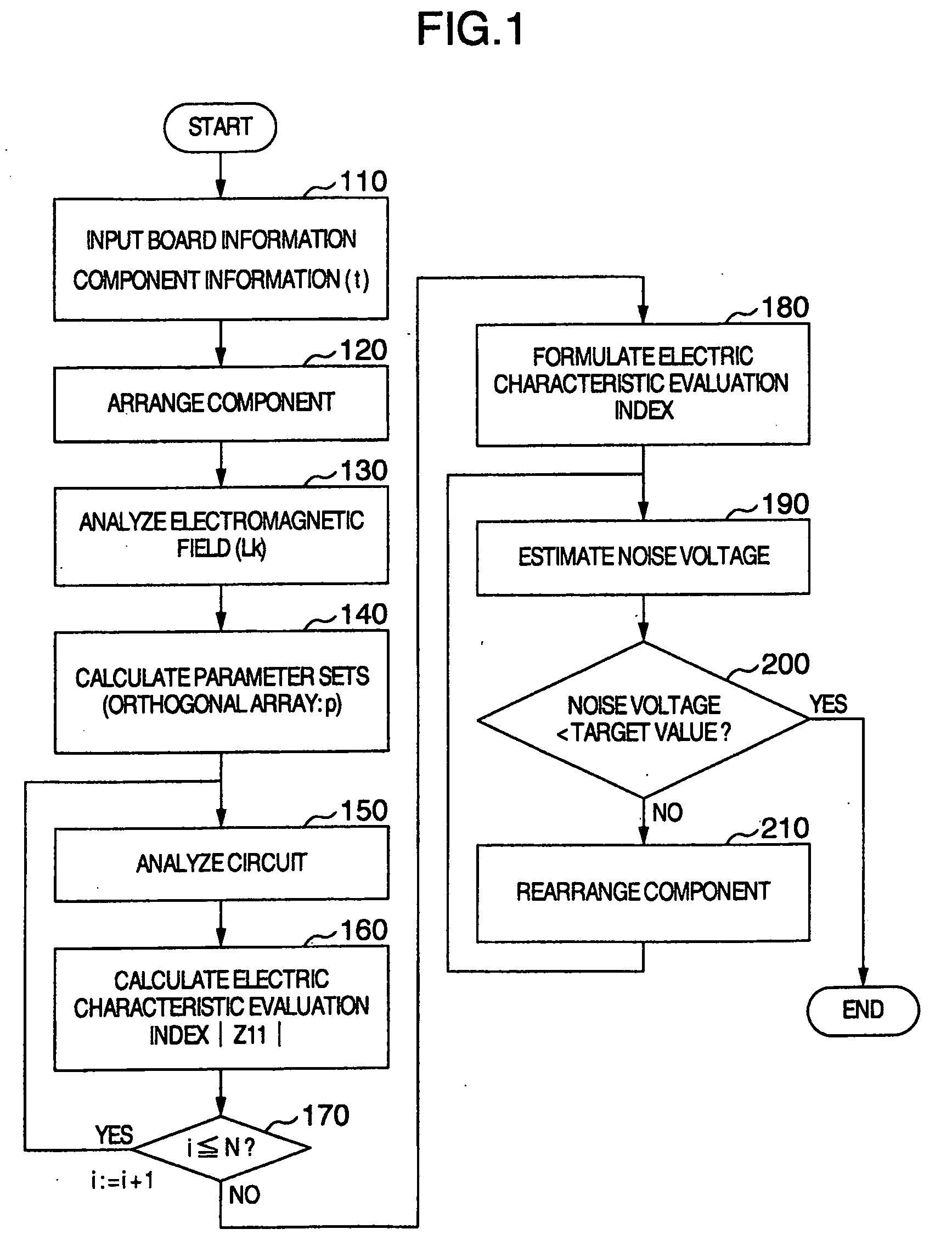
[0037]FIG. 1 is a flow chart illustrating a printed circuit board design method according to the invention. This flow chart will be described first, and then each process will be described in detail.

[0038]In a substrate information inputting process 110, design information of a printed circuit board necessary for printed circuit board design is input, including outer shape information of the printed circuit board, the number of layers, shape information of via holes and the like. At this stage, a wiring design rule and the like not shown are prepared in advance, including circuit connection information (net list), component list information, a wiring inhibition shortest distance, and the like. By using the net list and component list, a component arranging process 120 is executed. The component list includes information on each semiconductor device providing a function and information on each decoupling comp...

second embodiment

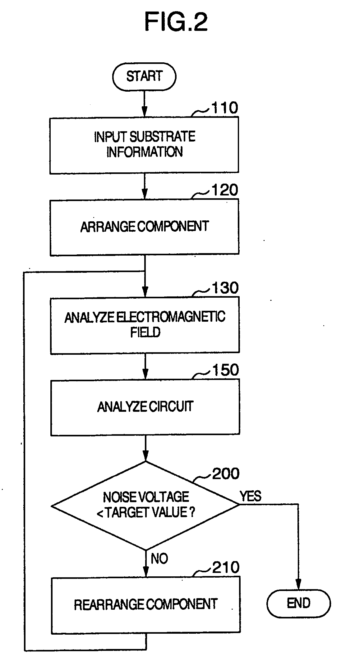
[0081]With reference to FIGS. 15, 16 and 17, the second embodiment will be described.

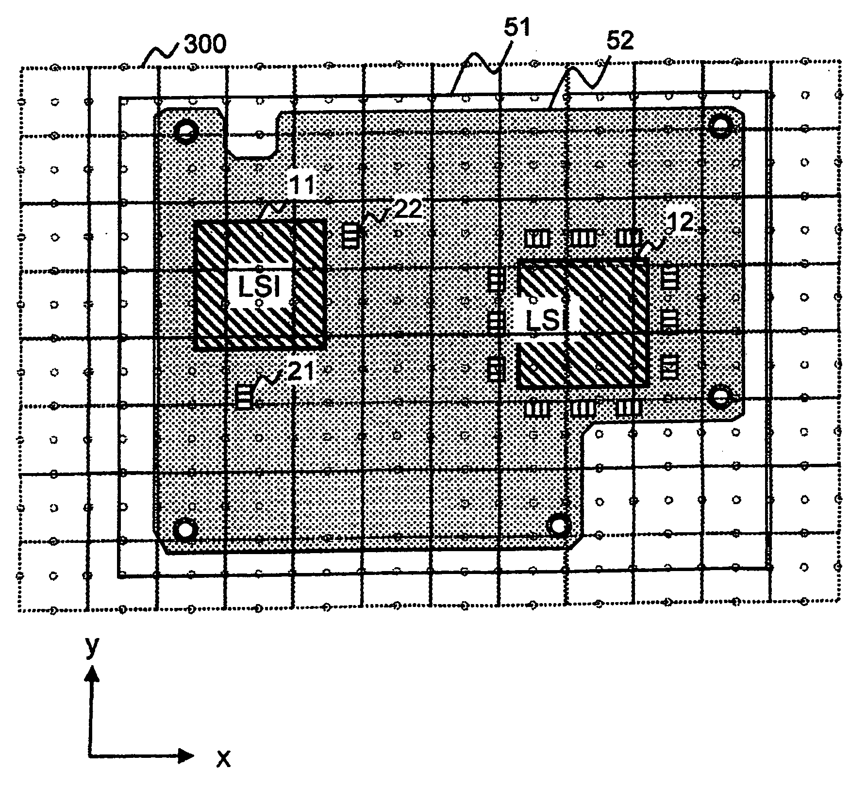
[0082]A different point of FIG. 15 from FIG. 1 resides in that a component rearranging process 230 is performed by using a graphical user interface (GUI). The detailed sequence of this process 230 is illustrated in FIG. 16. First, at Step 231, a noise voltage relative to component arrangement is estimated by using the estimation equation (1) similar to the first embodiment. Next, at Step 232, a calculation result is displayed as illustrated in FIG. 17. Namely, a working window 80 of an information processing apparatus constituting a design support system has screens of a board layout information area 81, an inductance information area 82 indicating a power source impedance and a waveform information area 83 indicating a voltage waveform. In the board information area 81, a power source layer pattern 52, semiconductor devices 11 and 12 and capacitors 21 and 22 are displayed in a printed circuit board...

third embodiment

[0087]The third embodiment will be described by using FIGS. 18 and 19. A difference from the first embodiment resides in that electromagnetic analysis at Step 130 calculates not the inductance Lk but a Y parameter. Instead of circuit analysis at Step 160, a matrix calculation (at Step 155) is performed. The Y parameter is an admittance parameter and uses an admittance matrix of Y parameters at each frequency in the target frequency range. By using Y parameters instead of circuit calculations, it becomes advantageous that formulation of the electric characteristic evaluation index through repetition of Steps 150 to 170 of the first embodiment can be performed in a short time.

[0088]Description will be made on the reason why the calculation is speeded up more that the circuit calculation, by using Y parameters.

[0089]First, description will be made on how a change in the power feeding system impedance when a capacitor component is replaced is calculated. With this calculation approach, ...


PUM


Abstract

An orthogonal array is formed by performing electromagnetic field analysis only once and determining a range by using the mount position and type of a capacitor and the number of capacitors as parameters to perform circuit analysis a small number of times. An estimation equation is formed by using as an index a result of the absolute value of the calculated power source impedance, and a capacitor is disposed to reduce noises by using the estimation equation.

Description

INCORPORATION BY REFERENCE[0001]The present application claims priority from Japanese application JP2008-039504 filed on Feb. 21, 2008, the content of which is hereby incorporated by reference into this application.BACKGROUND OF THE INVENTION[0002]The present invention relates to a printed circuit board noise calculating method and a design support apparatus using a CAD program for a printed circuit board having semiconductor devices and decoupling capacitors constituting an information processing apparatus such as a personal computer, a server, a router and a storage.[0003]Important guide lines for designing a printed circuit board include realizing functions provided by mounted components, reducing power source noises, reducing electromagnetic radiation from an apparatus, and the like. Reducing power source noises are particularly important from the viewpoint of ensuring stable operations of components mounted on a printed circuit board, such as semiconductor devices, analog devic...

Claims


Application Information

Patent Timeline
Patent Type & Authority Applications(United States)
IPC IPC(8): H05K1/18
CPCH05K1/0231H05K2201/093H05K3/0005
Inventor OSAKA, HIDEKIUEMATSU, YUTAKA
Owner HITACHI LTD
Why Eureka
Try Eureka