Apparatus for and method of forming carbon nanotube

Inactive Publication Date: 2009-08-27
DAINIPPON SCREEN MTG CO LTD
View PDF5 Cites 52 Cited by
  • Summary
  • Abstract
  • Description
  • Claims
  • Application Information

AI Technical Summary

Benefits of technology

[0028]It is therefore an object of the present invention to form a carbon nanotube of high quality with a high throughput.
[0029]It

Problems solved by technology

It is expected that current densities too high for copper to withstand will be required in the near future.
However, the conventionally attempted plasma CVD techniques are not capable of forming the carbon nanotube of sufficient quality as the BEOL wiring material.
From the viewpoint of industrial use, the conventional plasma CVD techniques have been impractical because of their low growth rate and low throughput.
The process executed in such two steps presents a significant problem in which, because the substrate with the metal na

Method used


Image

  • Apparatus for and method of forming carbon nanotube
  • Apparatus for and method of forming carbon nanotube
  • Apparatus for and method of forming carbon nanotube

Examples


Embodiment Construction

[0038]A preferred embodiment according to the present invention will now be described in detail with reference to the drawings.

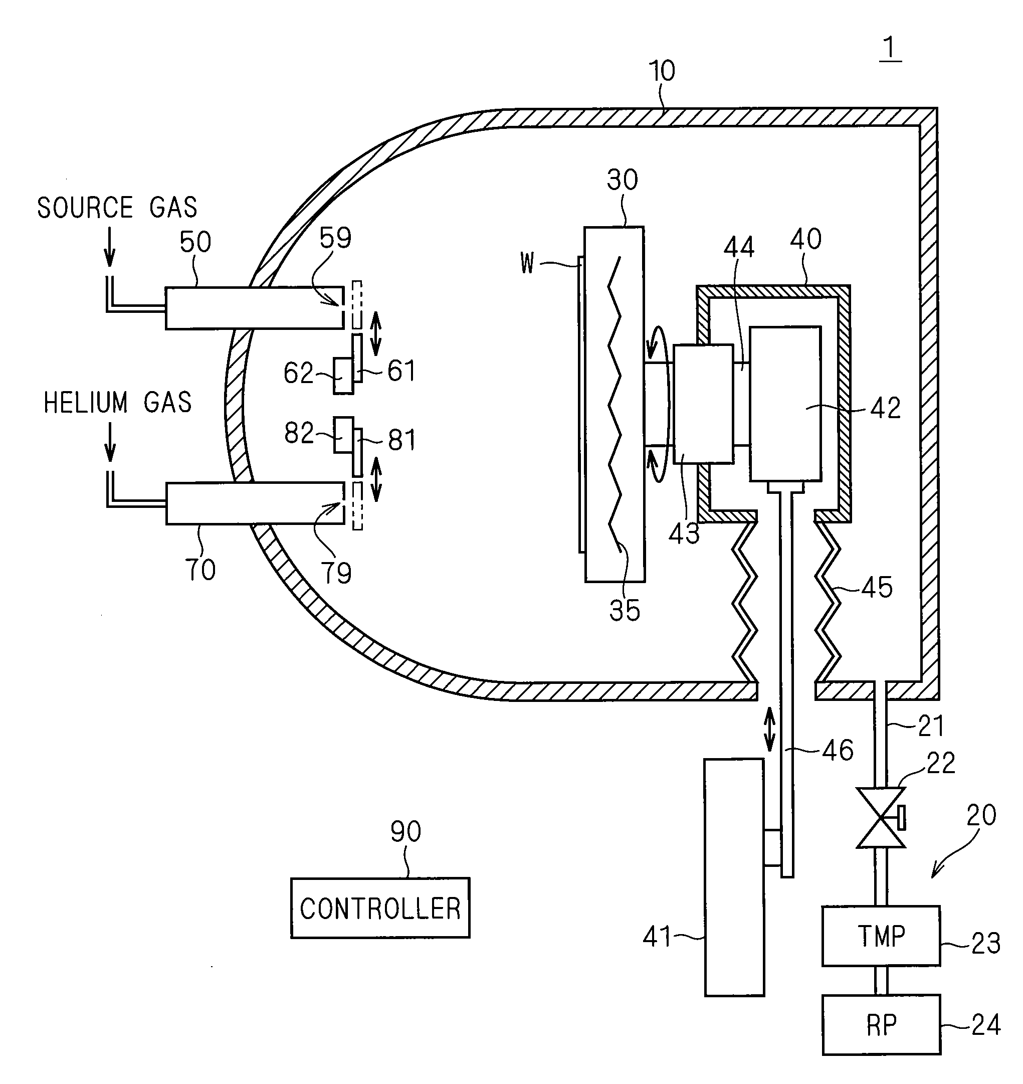
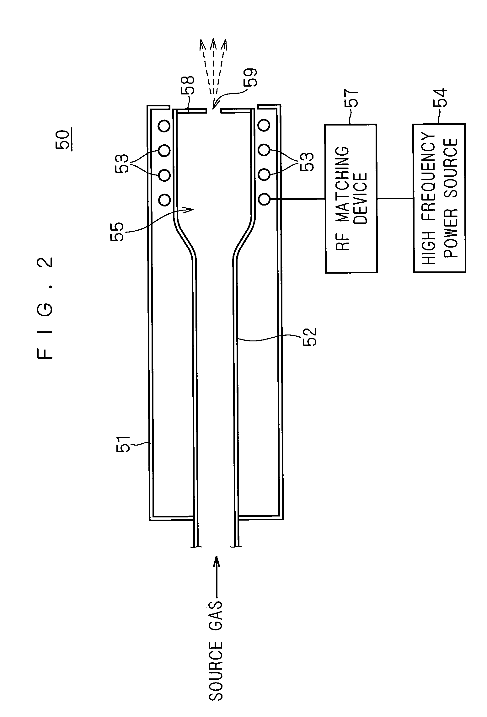
[0039]FIG. 1 is a view showing the overall construction of a carbon nanotube forming apparatus 1 according to the present invention. The carbon nanotube forming apparatus 1 according to the present invention is an apparatus for growing a carbon nanotube serving as a wiring material on a substrate such as a glass substrate for a liquid crystal display, for example, with a silicon film formed on the surface thereof, a semiconductor wafer, and the like. The carbon nanotube forming apparatus 1 is configured such that an evacuation mechanism 20, a substrate holding part 30, a radical beam irradiation part 50 and a nanoparticle beam irradiation part 70 are attached to a vacuum chamber 10. The carbon nanotube forming apparatus 1 further includes a controller 90 for controlling the operating mechanisms provided in the carbon nanotube forming apparatus 1 to execute t...


PUM

PropertyMeasurementUnit
Pressureaaaaaaaaaa
Pressureaaaaaaaaaa
Temperatureaaaaaaaaaa

Abstract

A vacuum chamber includes a radical beam irradiation part and a nanoparticle beam irradiation part. A substrate is held by a substrate holding part. The nanoparticle beam irradiation part irradiates the substrate with a beam of metal nanoparticles serving as a catalyst to form the catalyst on the substrate. Thereafter, the radical beam irradiation part generates a plasma from a source gas to irradiate the substrate with a beam of generated neutral radical species to grow a carbon nanotube on the substrate. The provision of an aperture in the radical beam irradiation part allows a relatively high degree of vacuum of 10−5 Torr to 10−3 Torr to be maintained in the vacuum chamber if the generation of the plasma involves a high pressure.

Description

BACKGROUND OF THE INVENTION[0001]1. Field of the Invention[0002]The present invention relates to an apparatus for and a method of forming a carbon nanotube which grow the carbon nanotube as a wiring material on a substrate such as a semiconductor wafer.[0003]2. Description of the Background Art[0004]In recent years, there has been a rapidly growing interest in an attempt to use a carbon nanotube as a BEOL (back-end-of-line) wiring material for LSI. Copper (Cu) has been generally used as a conventional wiring material. However, as patterns become finer for higher performance, current densities in wiring parts grow higher. It is expected that current densities too high for copper to withstand will be required in the near future. The carbon nanotube has a configuration such that a sheet of graphite (a graphene sheet) is rolled into a cylindrical shape, and has a diameter of several nanometers to tens of nanometers. It has been found that the carbon nanotube has very good electrical and...

Claims


Application Information

Patent Timeline
IPC IPC(8): C23C16/48
CPCB01J19/088H05H1/30B01J23/75B01J23/84B01J2219/0879B01J2219/0892B01J2219/0894B82Y30/00B82Y40/00C01B31/0226C01B31/0233C23C14/22C23C14/228C23C16/26C23C16/48B01J23/74C01B32/16C01B32/162B82B3/0004B82B3/0009
Inventor SAITO, KIMITSUGU
Owner DAINIPPON SCREEN MTG CO LTD
Why Eureka
Try Eureka