Organic electroluminescence element

a technology of electroluminescence element and organic material, applied in the direction of discharge tube/lamp details, discharge tube luminescnet screen, organic semiconductor device, etc., can solve the problems of large improvement in light-emission efficiency and drive durability, and the effect of lowering the driving voltag

Inactive Publication Date: 2009-09-03
UDC IRELAND
View PDF2 Cites 16 Cited by
  • Summary
  • Abstract
  • Description
  • Claims
  • Application Information

AI Technical Summary

Benefits of technology

[0277]It is clear from the results shown in Table 3 that the inventive element Nos. 11 to 16 have light-emission characteristics of unexpectedly high external quantum efficiency and low driving voltage. Further, the inventive element Nos. 13 to 16 have light-emission characteristics of further unexpectedly high external quantum efficiency, low driving voltage, and high drive durability. It is revealed that more excellent effects of the invention are obtained by using two of the compounds represented by formula (1) in combination.
[0278]Preparation of inventive organic EL element Nos. 22 to 24 and comparative element C1 was conducted in a similar manner to that in the process in the preparation of the organic EL elements of

Problems solved by technology

For the practical application of an organic EL element, however, there are still many problems such as improvements in light-emission efficiency and drive durability.
However, as an electron transportability and hole transportability by the electron transporting material and hole transporting material which act as a host are insufficient, improvement in light-emission efficiency and lowering of driving voltage are not obtained as expected.
However, since the adamantane compound does not have charge transportability, charges flow only on the guest compound.
Accordingly, the driving voltage is increased by incorporating the adamantane compound, and as a result, a large improvement in the light-emission efficiency is not expected.

Method used


Image

  • Organic electroluminescence element
  • Organic electroluminescence element
  • Organic electroluminescence element

Examples


example 1

1. Preparation of Organic EL Element

[0233](Preparation of Comparative Organic EL Element A1)

[0234]1) Formation of Anode

[0235]As a transparent substrate, the one in which indium tin oxide (which is referred to hereinafter as ITO) was deposited on a glass substrate having a size of 25 mm×25 mm×0.7 mm to form a film having a thickness of 100 nm (manufactured by Tokyo Sanyo Vacuum Co., Ltd.) was used. The transparent substrate was subjected to etching and cleaning.

[0236]2) Hole Injection Layer and Hole Transport Layer

[0237]On the resulting ITO glass substrate, copper phthalocyanine (which is referred to hereinafter as CuPc) was deposited at a thickness of 10 nm, and then, N,N′-dinaphthyl-N,N′-diphenyl-[1,1′-biphenyl]-4,4′-diamine (which is referred to hereinafter as α-NPD) was deposited at a thickness of 50 nm.

[0238]3) Light-Emitting Layer

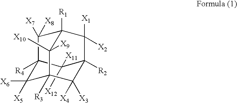
[0239]On the hole injection layer and hole transport layer, compound (AD-1) of formula (1) and platinum complex Pt-1 as an electron-transporting light...

example 2

1. Preparation of Sample

[0267](Preparation of Organic EL Element No. 5)

[0268]Preparation of inventive organic EL element No. 5 was conducted in a similar manner to the process in the preparation of the organic EL element No. 1 of Example 1, except that, in the preparation of the organic EL element No. 1 of Example 1, the following layer was used as the light-emitting layer.

[0269]Ternary element co-deposition was conducted using hole-transporting host material mCP, compound (AD-2) of formula (1), and electron-transporting light-emitting material Pt-1, so that the weight ratio of mCP:AD-2:Pt-1 would be 70:15:15. The deposition thickness was 30 nm.

[0270](Preparation of Organic EL Element No. 6)

[0271]Preparation of inventive organic EL element No. 6 was conducted in a similar manner to the process in the preparation of the organic EL element No. 1 of Example 1, except that, in the preparation of the organic EL element No. 1 of Example 1, the following layer was used as the light-emittin...

example 3

1. Preparation of Organic EL Element Nos. 11 to 16

[0275]Preparation of inventive organic EL element Nos. 11 to 16 was conducted in a similar manner to that in the process in the preparation of the organic EL element No. 3 of Example 1, except that, in the preparation of the organic EL element No. 3 of Example 1, the compound(s) shown in Table 3 was (were) used as the compound of formula (1) in the light-emitting layer with the mixing ratio shown in Table 3. In each element, the content of the light emitting material Pt-1 was kept constant to be 15% by weight. In Table 3, when the total amount of the compounds of formula (1) exceeds 35% by weight, the content of the host material mCP is reduced for adjustment.

2. Performance Evaluation

[0276]Concerning the obtained elements, performance was evaluated in a similar manner to that in Example 1. Results are shown in Table 3.

[0277]It is clear from the results shown in Table 3 that the inventive element Nos. 11 to 16 have light-emission cha...


PUM


Abstract

An organic electroluminescence element having at least one organic compound layer including a light-emitting layer, which is disposed between a pair of electrodes, wherein the light-emitting layer includes a light emitting material, a compound represented by the following formula (1) and a charge transporting material. An organic EL element that exhibits high light-emission efficiency and low driving voltage, and is excellent in drive durability is provided.

Description

CROSS-REFERENCE TO RELATED APPLICATION [0001]This application claims priority under 35 USC 119 from Japanese Patent Application Nos. 2008-48628 and 2008-315024, the disclosures of which are incorporated by reference herein.BACKGROUND OF THE INVENTION[0002]1. Field of the Invention[0003]The present invention relates to an organic electroluminescence element (hereinafter, referred to as an “organic EL element” in some cases, and also referred to as an organic light emitting diode (OLED)) which can be effectively applied to a surface light source for full color displays, backlights, illumination light sources and the like; or a light source array for printers and the like.[0004]2. Description of the Related Art[0005]An organic EL element is composed of a light-emitting layer or a plurality of organic layers containing a light-emitting layer, and a pair of electrodes sandwiching the organic layers. The organic EL element is an element for obtaining luminescence by utilizing at least eit...

Claims


Application Information

Patent Timeline
Patent Type & Authority Applications(United States)
IPC IPC(8): H01J1/63
CPCC09K11/06C09K2211/1003C09K2211/185H10K85/60H10K85/346H10K85/342H10K85/6572H10K50/11H10K2101/10H10K2101/30
Inventor SOTOYAMA, WATARUSHIBATA, KAZUYUKITOBISE, MANABUTAKEDA, AKIRA
Owner UDC IRELAND
Why Eureka
Try Eureka