

Solid-state imaging apparatus, method of driving solid-state imaging apparatus, and imaging system
- Summary
- Abstract
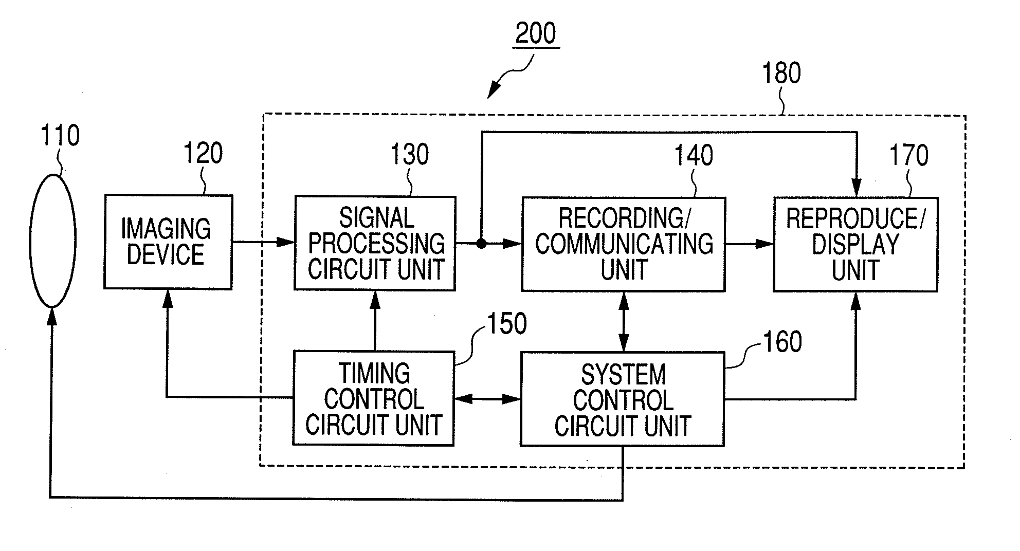
- Description
- Claims
- Application Information
AI Technical Summary
Benefits of technology
Problems solved by technology
Method used
Image

Examples
first embodiment
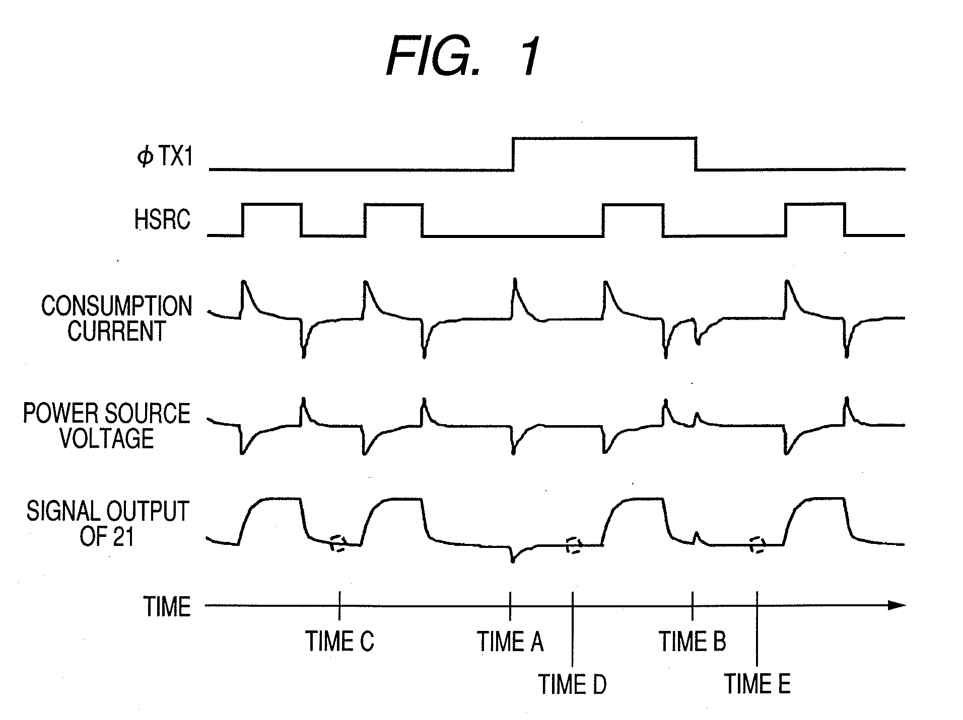
[0026]As a method of addressing the solve problem, there can be used a technique which holds horizontal scanning signal HSRC at a high level or a low level around a time when consumption current / power source voltage fluctuation not synchronized with the periodicity of horizontal scanning signal HSRC occurs, so that the horizontal scanning signal HSRC pulse is stopped. With this technique, it is possible to avoid peculiar consumption current / power source voltage fluctuation caused by a drive signal other than horizontal scanning signal HSRC. In this case, however, it was further found that the periodicity of consumption current / power source voltage fluctuation caused by the horizontal scanning signal HSRC pulse is not kept, thus causing noise.
[0027]The method of driving a solid-state imaging apparatus will be described with reference to FIG. 1. Referring to FIG. 1, when the horizontal scanning signal HSRC pulse being the clock pulse is stopped, the noise dependent on peculiar consump...
second embodiment
[0036]A solid-state imaging apparatus according to a second embodiment of the present invention will be described with reference to FIGS. 8 and 9. FIG. 8 illustrates an equivalent circuit corresponding to the horizontal scanning circuit of FIG. 2; in other aspects, including the reading from the pixel to the capacitor, the configuration is the same as that of the first embodiment. FIG. 9 is a drive timing chart.
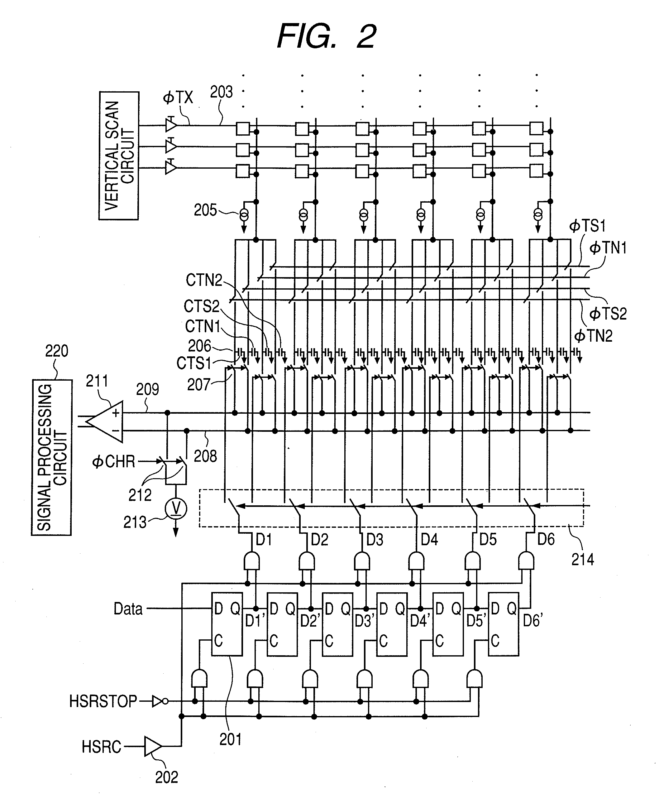
[0037]A clock buffer 802 performs waveform shaping of horizontal scanning signal HSRC and outputs the signal. An AND of the output signal from the clock buffer 802 and an logically inverted signal of signal HSRSTOP is calculated, and the calculated AND is input to the clock input terminal C of the flip-flop 801. The flip-flop 801 outputs data D1′, D2′, D3′, D4′, in this order in synchronization with the rising edge of the input signal to the clock input terminal C. More specifically, during a period when signal HSRSTOP is at low level, the flip-flop 801 shifts the high level ...
third embodiment
[0039]A solid-state imaging apparatus according to a third embodiment of the present invention will be described with reference to FIG. 10. FIG. 11 is a waveform diagram for describing the operation of the solid-state imaging apparatus of FIG. 10. Reference numeral 1001 denotes a flip-flop constituting the horizontal scanning circuit. The horizontal scanning circuit further includes a clock buffer 1002, terminal HSRSTOP being a mask signal input portion, and AND gate. The clock buffer 1002 performs waveform shaping of horizontal scanning signal HSRC. Reference numeral 1003 denotes a pixel; 1005 a constant current load; 1006 a capacitor for temporarily saving a pixel signal; 1007 a switch for connecting the capacitor 1006 to horizontal common lines 1008 and 1009 and thereby reading out the signal. An amplifier 1011 being a differential processing circuit outputs a differential signal between the signal output to the horizontal common line 1008 and the signal output to the horizontal ...
PUM
 Abstract
Description
Claims
Application Information