Display device

a display device and display technology, applied in the field of display devices, can solve the problems of difficulty in correctly aligning the pixel electrodes and color filters, affecting the uniformity of cell gaps throughout the display device, and generating alignment errors, so as to improve the step coverage of the overlapping portions of the color filters and prevent the non-uniformity of parasitic capacitance of pixels

Inactive Publication Date: 2009-09-10
SAMSUNG DISPLAY CO LTD
View PDF7 Cites 36 Cited by
  • Summary
  • Abstract
  • Description
  • Claims
  • Application Information

AI Technical Summary

Benefits of technology

[0031]Accordingly, the data lines are formed away from the overlapping portions of the color filter such that the increasing of the step coverage of the overlapping portions of the color filter may be prevented, thereby forming a uniform cell gap. The data line and the light-blocking member may prevent

Problems solved by technology

However, in such LCDs the pixel electrodes and color filters are respectively formed on different display panels in the LCD such that it is difficult to correctly align the pixel electrodes and color filters, and as a result an alignment error may be generated.
Accordingly, the

Method used


Image

  • Display device
  • Display device
  • Display device

Examples


exemplary embodiment 1

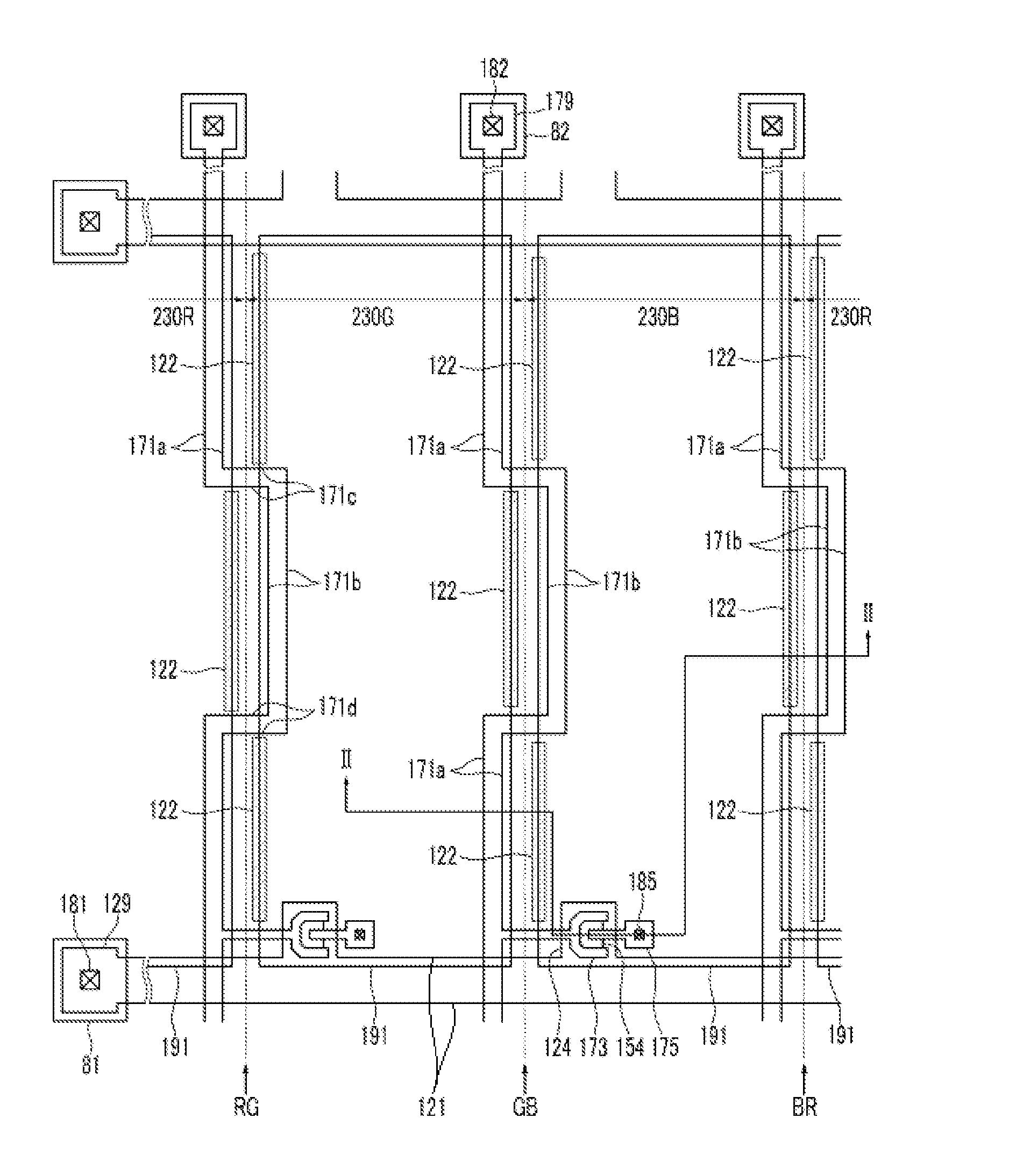
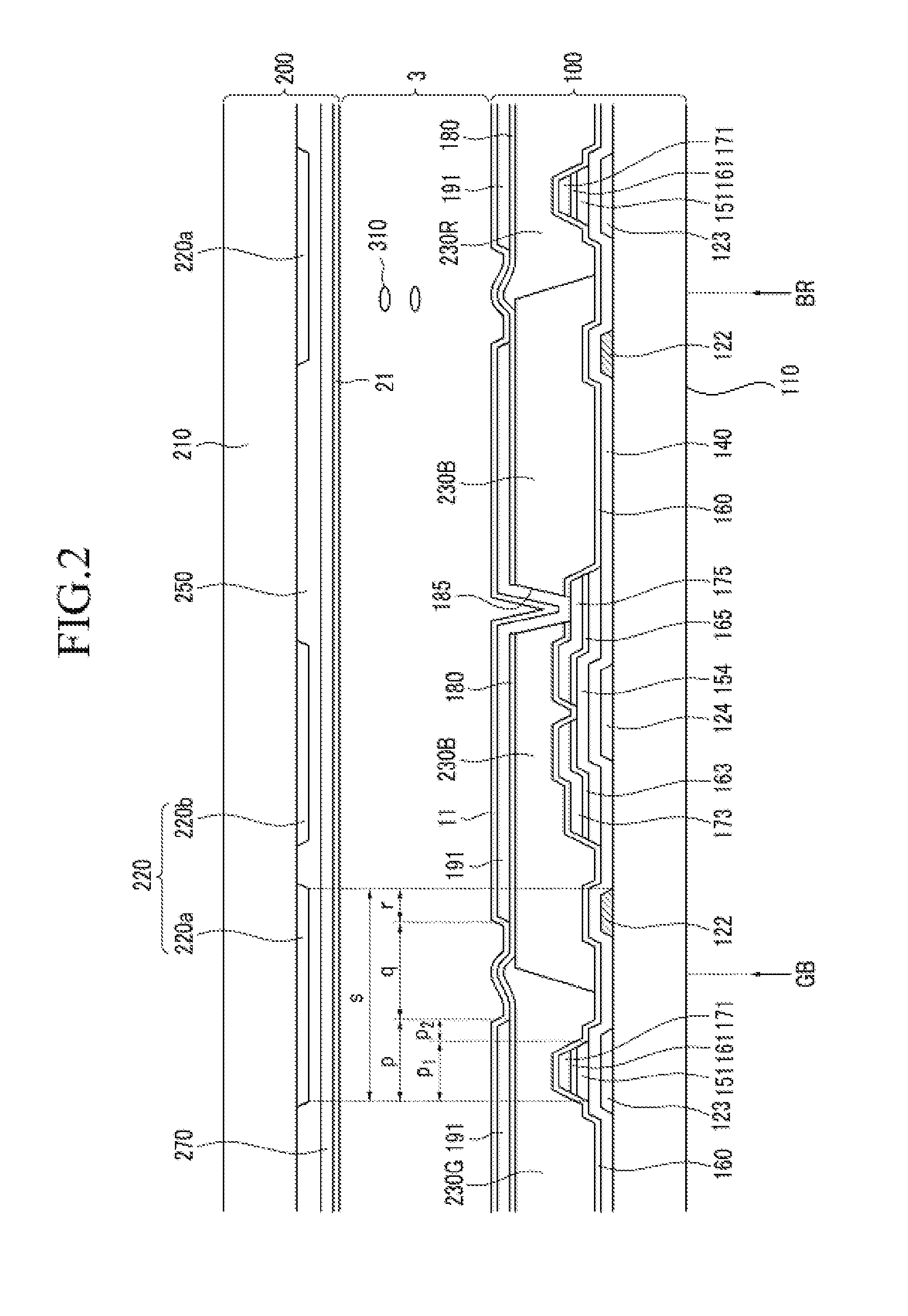
[0047]Firstly, an exemplary embodiment of a liquid crystal display (“LCD”) according to the present invention will be described with the reference to FIG. 1 and FIG. 2.

[0048]FIG. 1 is a top plan layout view illustrating an exemplary embodiment of two neighboring pixels in an exemplary embodiment of an LCD according to the present invention, and FIG. 2 is a cross-sectional view of the exemplary embodiment of an LCD of FIG. 1 taken along line II-II.

[0049]Referring to FIG. 1 and FIG. 2, the exemplary embodiment of an LCD according to the present invention includes a thin film transistor (“TFT”) array panel 100, a common electrode panel 200 facing the thin film transistor array panel 100 and a liquid crystal layer 3 interposed between the thin film transistor array panel 100 and the common electrode panel 200.

[0050]Hereinafter, the TFT array panel 100 will be described. A gate conductor including a plurality of gate lines 121, a plurality of first light-blocking members 122, and a plura...

exemplary embodiment 2

[0091]Next, a second exemplary embodiment of an LCD according to the present invention will be described with reference to drawings. Each pixel of the present exemplary embodiment includes a pair of sub-pixels, different from the above-described exemplary embodiment. Descriptions repeating the previous exemplary embodiment are omitted, and the same constituent elements are indicated by the same reference numerals.

[0092]FIG. 3 is an equivalent circuit diagram of an exemplary embodiment of one pixel of an exemplary embodiment of an LCD according the present invention.

[0093]Referring to FIG. 3, an exemplary embodiment of an LCD includes a plurality of signal lines having a plurality of pairs of gate lines 121a and 121b, a plurality of data lines 171, and a plurality of storage electrode lines 131, and a plurality of pixels PX connected thereto.

[0094]Each pixel PX has a pair of sub-pixels PXa and PXb. Each sub-pixel PXa / PXb has a switching element Qa / Qb connected to a corresponding gate...


PUM


Abstract

A display device includes; a first substrate, a first pixel electrode disposed on the first substrate, a second pixel electrode disposed on the first substrate and neighboring the first pixel electrode, a first color filter disposed under the first pixel electrode, a second color filter disposed under the second pixel electrode and overlapping the first color filter in an area between the first pixel electrode and the second pixel electrode, and a data line including a first portion and a second portion respectively disposed on left and right sides of the area wherein the first and second color filters overlap.

Description

[0001]This application claims priority to Korean Patent Application No. 10-2008-0021668, filed on Mar. 7, 2008, and all the benefits accruing therefrom under 35 U.S.C. §119, the contents of which in its entirety are herein incorporated by reference.BACKGROUND OF THE INVENTION[0002](a) Field of the Invention[0003]The present invention relates to a display device.[0004](b) Description of the Related Art[0005]Liquid crystal displays (“LCDs”) are one of the most widely used flat panel displays. An LCD typically includes a pair of panels provided with field-generating electrodes, such as pixel electrodes and a common electrode, and a liquid crystal (“LC”) layer interposed between the two panels. The LCD displays images by applying voltages to the field-generating electrodes to generate an electric field in the LC layer that determines orientations of LC molecules therein to adjust polarization of incident light, and thereby adjust transmission of light through the display.[0006]In some t...

Claims


Application Information

Patent Timeline
IPC IPC(8): G09G3/36
CPCG02F1/133514G02F2001/136222G02F1/136286G02F1/136222G02F1/1335G02F1/1343
Inventor KIM, DONG-GYULEE, SEONG-YOUNG
Owner SAMSUNG DISPLAY CO LTD
Why Eureka
Try Eureka