Method for forming periodic structure

a technology of periodic structure and forming method, which is applied in the field of forming periodic structure, can solve the problems of low production rate, high cost of equipment for forming photonic crystal, and the inability to mass produce and apply photonic crystals

Active Publication Date: 2009-09-10
NAT TAIWAN UNIV
View PDF3 Cites 4 Cited by
  • Summary
  • Abstract
  • Description
  • Claims
  • Application Information

AI Technical Summary

Problems solved by technology

The equipment for forming photonic crystals are very expensive and have low production rates, such that photonic crystals are yet to be mass produced and applied.

Method used


Image

  • Method for forming periodic structure
  • Method for forming periodic structure
  • Method for forming periodic structure

Examples


example

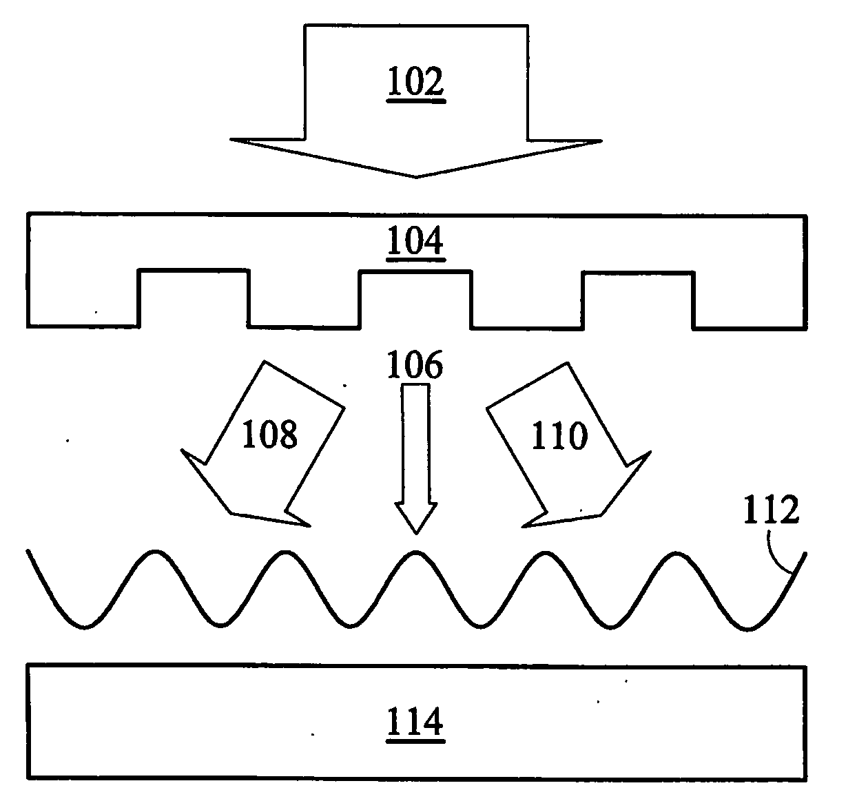
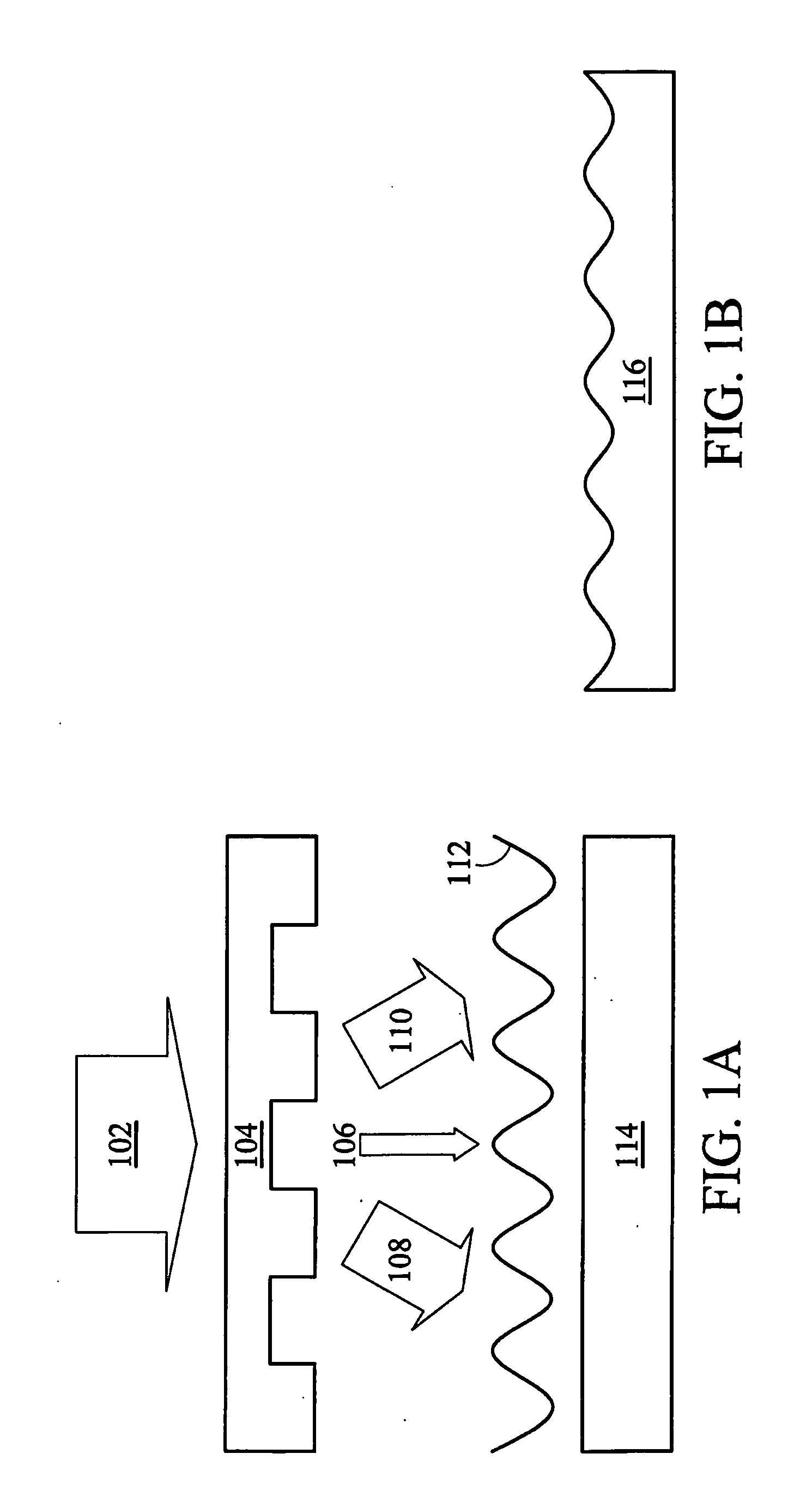
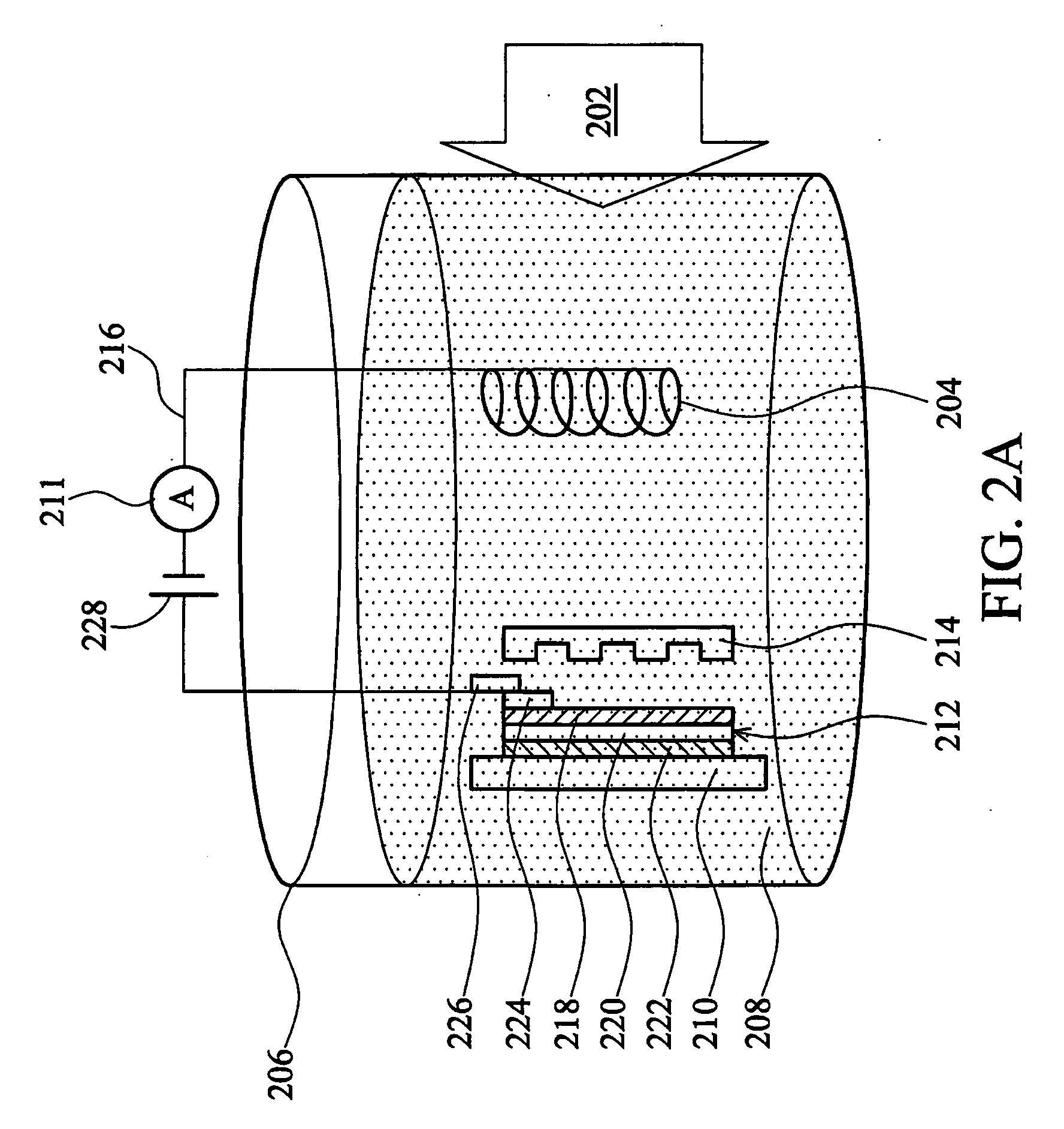
[0018]An example and related experiment data is described in the following paragraph to further illustrate the invention. A device is immersed into a KOH solution, which is used as an electrolyte. A Ti / Au layer with thickness of about 12 nm / 180 nm is formed on the p-GaN layer of the device to act as a p-type electrode. An Ni / Au layer with thickness of about 30 nm / 120 nm is formed on the n-GaN layer of the device to act as a p-type electrode. The semiconductor device is applied with a 0.7V negative bias and irradiated by a He—Cd laser passing through a phase mask to perform a photoelectrochemical etching process, in which interference strips are generated and are used as UV writing beams to pattern the p-GaN layer to form a grating structure.

[0019]FIG. 3 shows comparison of the light-emitting diode of the example and a conventional light-emitting diode. As shown in FIG. 3, the light-emitting device etched by the PEC to a depth of about 35 nm presents greater optical output energy tha...


PUM

PropertyMeasurementUnit
sizeaaaaaaaaaa
sizeaaaaaaaaaa
sizeaaaaaaaaaa

Abstract

A method for forming a periodic structure is disclosed. A structural layer and an optical modulation element are provided. A light is emitted to pass through the optical modulation element to irradiate interference strips on the structural layer. A photoelectrochemical etching (PEC) is performed to form the periodic structure according the interference strips irradiated on the structural layer.

Description

BACKGROUND OF THE INVENTION[0001]1. Field of the Invention[0002]The invention relates to a method for forming a periodic structure, such as photonic crystal, and more particularly relates a method for forming a periodic structure in a light-emitting device.[0003]2. Description of the Related Art[0004]Optoelectronic technology has rapidly developed, and is currently in wide usage, thus improving the wellbeing of mankind.[0005]In recent years, due to structure and process development of photonic crystals, application potential for photonic crystals has increased. Basically, photonic crystal is a structure with a periodic varying refractive index or dielectric constant and simulates arrangement of atoms in a solid crystal. Photonic crystals are similar to the energy gap of electrons in solid crystals and generates energy gap of photons therein. Hence, transmissive characteristics of electromagnetic waves, such as amplitude, phase, polarization or wavelength, can be changed by adjusting...

Claims


Application Information

Patent Timeline
Patent Type & Authority Applications(United States)
IPC IPC(8): H01L21/02
CPCH01L2933/0083H01L33/20
Inventor YANG, CHIH-CHUNGCHEN, CHENG-YENLIN, CHENG-HUNGYEH, DONG-MING
Owner NAT TAIWAN UNIV
Why Eureka
Try Eureka