Fabricating a silicon carbide and nitride structures on a carrier substrate

a technology of silicon carbide and nitride, which is applied in the field of semiconductor structures, can solve the problems of less than desired quality of thin-film devices formed on silicon carbide and group iii nitrides than other materials such as silicon, and the difficulty of fabricating devices on silicon carbide structures,

Active Publication Date: 2022-06-14
THE BOEING CO
View PDF4 Cites 0 Cited by
  • Summary
  • Abstract
  • Description
  • Claims
  • Application Information

AI Technical Summary

Problems solved by technology

Fabricating devices on silicon carbide structures can be challenging.
For example, the devices formed using thin-films with silicon carbide and group III nitrides can be more difficult to fabricate than desired as compared to other materials such as silicon.
The quality of thin-film devices using silicon carbide and group III nitrides formed on a wafer may not be as great as desired as compared to materials such as silicon.

Method used


Image

  • Fabricating a silicon carbide and nitride structures on a carrier substrate
  • Fabricating a silicon carbide and nitride structures on a carrier substrate
  • Fabricating a silicon carbide and nitride structures on a carrier substrate

Examples


Embodiment Construction

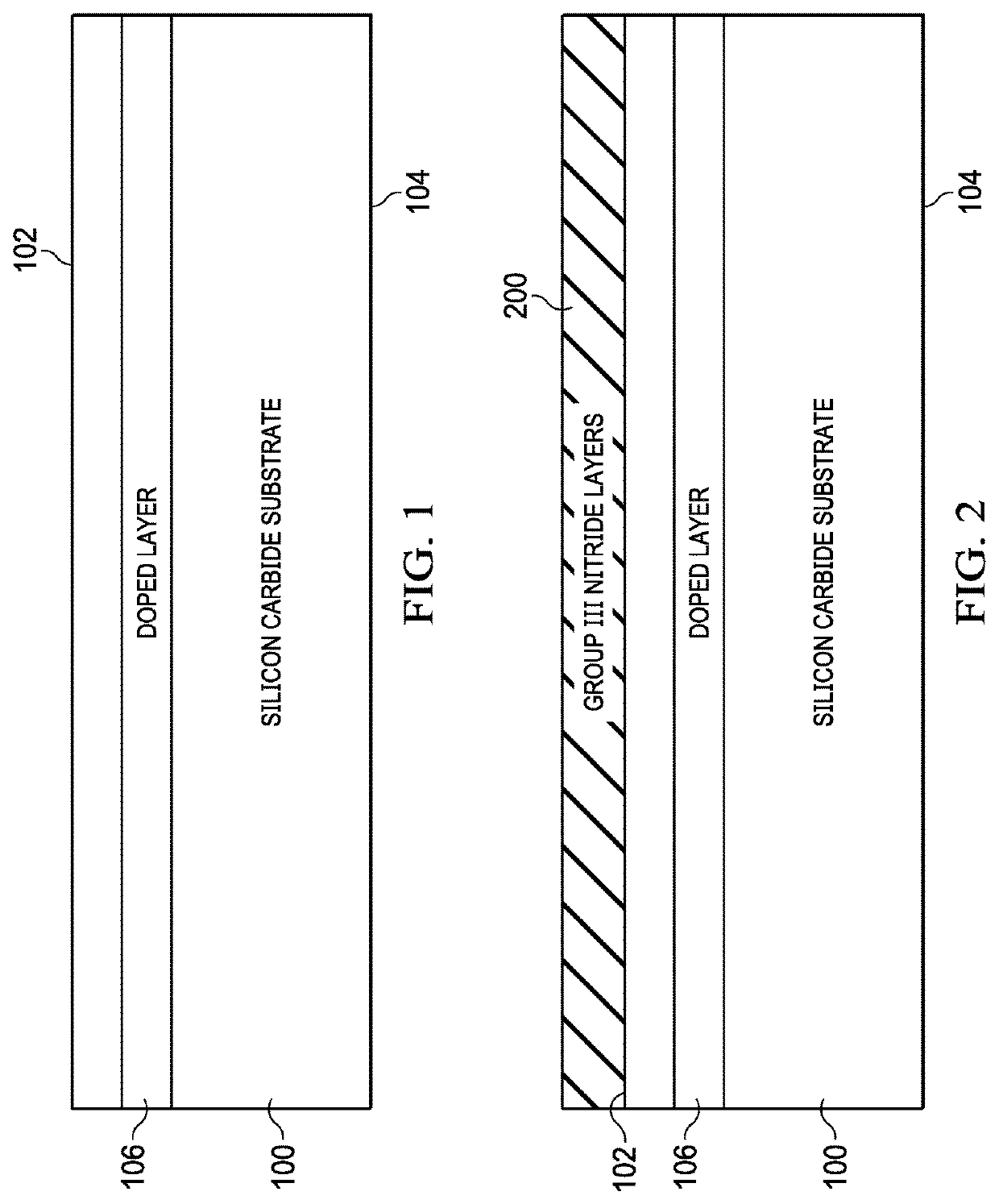
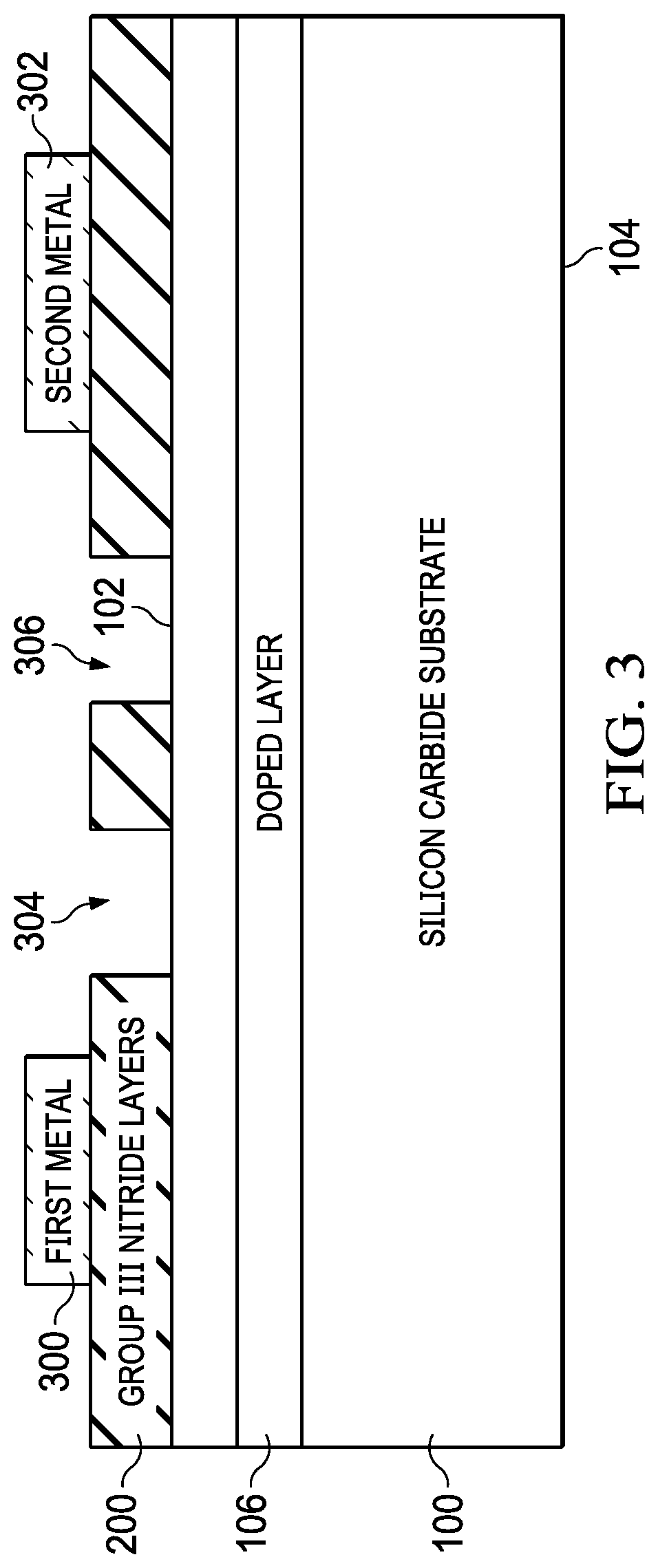
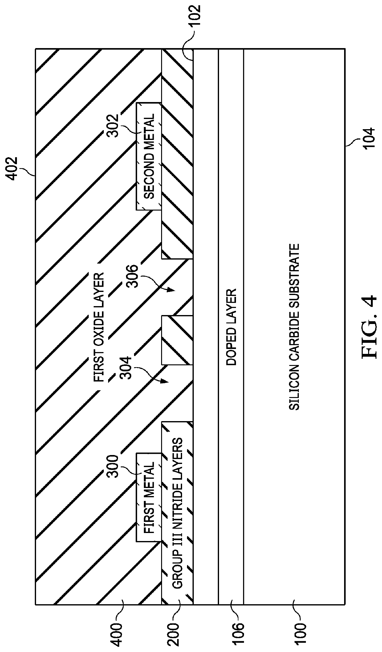
[0041]The illustrative embodiments recognize and take into account one or more different considerations. For example, the illustrative embodiments recognize and take into account that currently used techniques can yield polycrystalline films of non-uniform silicon carbide across a wafer. Further, the illustrative embodiments recognize and take into account that when using current techniques to obtain a desired thickness for thin-film devices, material damage can occur in a silicon carbide film, thus leading to undesired optical absorption or scattering.

[0042]Further, the illustrative embodiments recognize and take into account that current techniques for fabricating silicon carbide (SiC) nano-photonics have primarily been restricted to 3C-SiC (cubic crystal structure) that is epitaxially grown on silicon (Si). The illustrative embodiments recognize and take into account that while 3C-SiC is simple to undercut on Si or silicon dioxide (SiO2) because of the chemical etch selectivity b...


PUM

PropertyMeasurementUnit
areaaaaaaaaaaa
thicknessaaaaaaaaaa
thickaaaaaaaaaa

Abstract

A method, apparatus, and system for forming a semiconductor structure. A first oxide layer located on a set of group III nitride layers formed on a silicon carbide substrate is bonded to a second oxide layer located on a carrier substrate to form an oxide layer located between the carrier substrate and the set of group III nitride layers. The silicon carbide substrate has a doped layer. The silicon carbide substrate having the doped layer is etched using a photo-electrochemical etching process, wherein a doping level of the doped layer is such that the doped layer is removed and a silicon carbide layer in the silicon carbide substrate remains unetched. The semiconductor structure is formed using the silicon carbide layer and the set of group III nitride layers.

Description

CROSS-REFERENCE TO RELATED APPLICATION[0001]This application is related to the following patent application: entitled “Silicon Carbide and Nitride Structures on a Substrate”, Ser. No. 16 / 874,619, filed May 14, 2020, which published as U.S Publication No. US-2021-0356658-A1, on Nov. 18, 2021, assigned to the same assignee, and incorporated herein by reference.BACKGROUND INFORMATION1. Field[0002]The present disclosure relates generally to semiconductors and, in particular, to a method for forming semiconductor structures and, in particular, to forming silicon carbide and nitride structures on a carrier substrate.2. Background[0003]Silicon carbide and group III nitrides, such as gallium nitride, are desirable semiconductors for signal processing and quantum applications. These materials have wide bandgaps greater than 3 eV and greater nonlinear optical coefficients as compared to other material such as silicon, silica, and silicon nitride materials currently used for low-loss photonics...

Claims


Application Information

Patent Timeline
Patent Type & Authority Patents(United States)
IPC IPC(8): H01L21/02H01L21/04
CPCH01L21/02378H01L21/02013H01L21/02458H01L21/0475G02F1/355G02F1/3556H01L21/02002H01L21/2007H01L21/7605H01L21/76275H01L21/3063H01L21/0445H01L29/66053H01L29/1608H01L21/02447H01L21/0254H01L21/02664
Inventor WHITELEY, SAMUEL J.YAP, DANIELCHEN, EDWARD H.KIM, DANNY M.LADD, THADDEUS D.
Owner THE BOEING CO
Why Eureka
Try Eureka