A method of manufacturing a vertical light-emitting diode chip
A light-emitting diode and chip technology, applied in semiconductor devices, electrical components, circuits, etc., can solve the problems of epitaxial wafer damage and low yield rate
- Summary
- Abstract
- Description
- Claims
- Application Information
AI Technical Summary
Problems solved by technology
Method used
Image
Examples
Embodiment Construction
[0030] In order to make the object, technical solution and advantages of the present invention clearer, the present invention will be described in further detail below in conjunction with specific embodiments and with reference to the accompanying drawings.
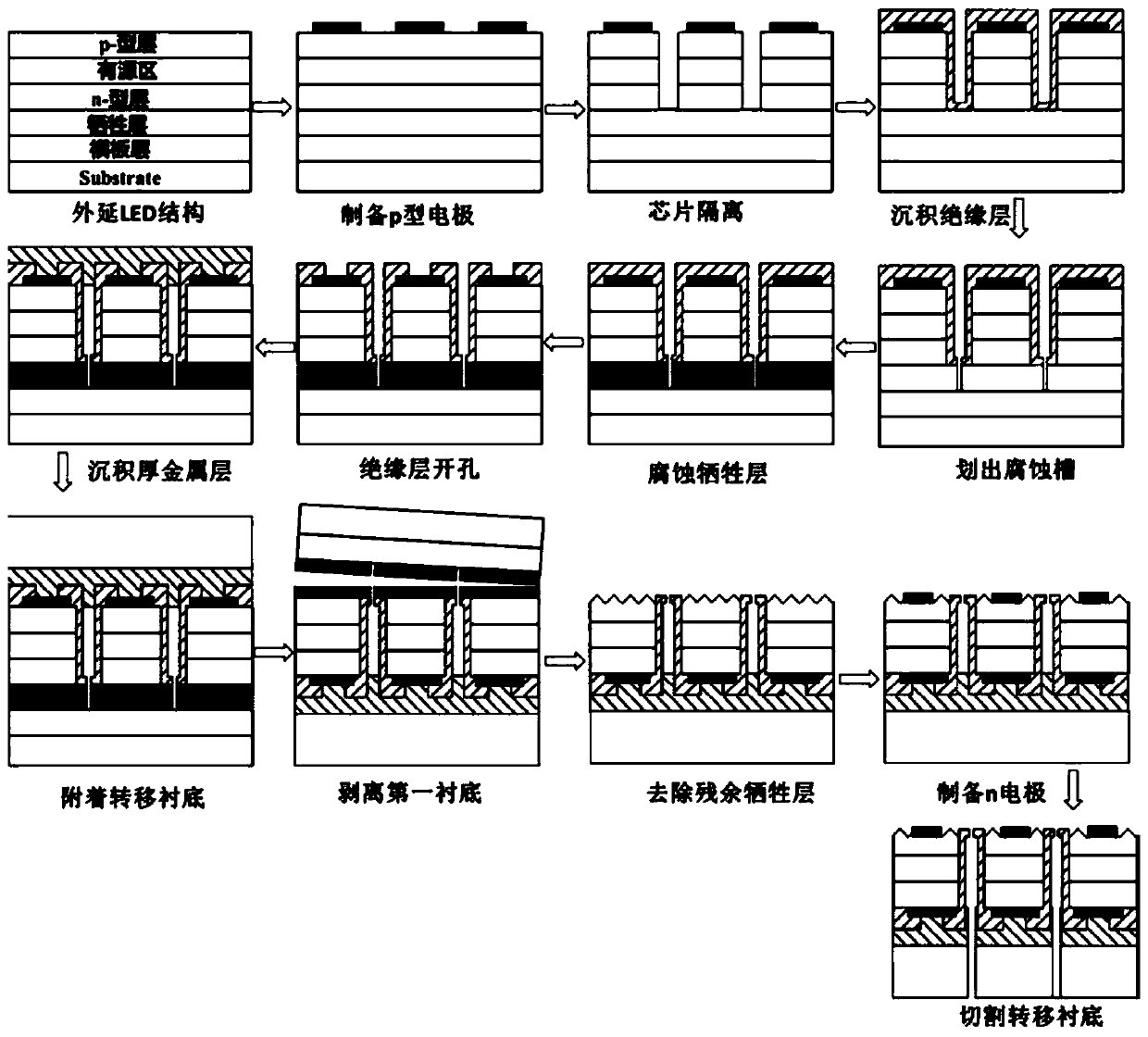
[0031] Vertical structure LED chip preparation method of the present invention, such as figure 1 As shown, it mainly includes the following steps:
[0032] Step 1. Epitaxial LED structure: On the first substrate, there are epitaxial template layer, sacrificial layer, n-type layer, active region and p-type layer sequentially from the substrate upward.
[0033] When selecting the first substrate, it should be considered that the crystal structure of the substrate material and the epitaxial material is the same or similar, the thermal expansion coefficient should match, and the substrate material should have good chemical stability. It should not be decomposed and corroded in the temperature and atmosphere of epitaxial growt...
PUM
| Property | Measurement | Unit |
|---|---|---|
| thickness | aaaaa | aaaaa |
| emission peak | aaaaa | aaaaa |
Abstract
Description
Claims
Application Information

