Circuit and Method for a Vdd Level Memory Sense Amplifier

a memory sense amplifier and circuit technology, applied in information storage, static storage, digital storage, etc., can solve the problems of cell disturb, limited vdd minimum power supply, and low signal quality, so as to improve the operation of sense amplifiers and high-speed sense amplifier operations.

Active Publication Date: 2009-09-17
TAIWAN SEMICON MFG CO LTD
View PDF6 Cites 14 Cited by
  • Summary
  • Abstract
  • Description
  • Claims
  • Application Information

AI Technical Summary

Benefits of technology

[0018]These and other problems are generally solved or circumvented, and technical advantages are generally achieved, by embodiments of the present invention, which provide circuits and methods to improve the operation of sense amplifiers and the voltage references used with the sense amplifiers without requiring dummy cells or added write select signals to enable high speed sense amplifier operations.

Problems solved by technology

These area requirements negatively affect the packing density (by increasing the silicon area used per memory storage bit) and are thus undesirable in applications where silicon area is a critical factor, such as in embedded DRAM applications.
As is known in the art, the need for reliable operation of DRAM cells in advanced semiconductor processes may limit the minimum power supply Vdd that can be used.
Cell disturb problems are also known in the prior art, as feature sizes are reduced in smaller and smaller technologies.
However, it is also known that this approach can lead to cell disturb errors.
In cell disturb errors, cells on non-selected bit lines can have their stored charge altered, creating an erroneous memory read operation in future cycles.

Method used


Image

  • Circuit and Method for a Vdd Level Memory Sense Amplifier
  • Circuit and Method for a Vdd Level Memory Sense Amplifier
  • Circuit and Method for a Vdd Level Memory Sense Amplifier

Examples


Embodiment Construction

[0040]The making and using of the presently preferred embodiments are discussed in detail below. It should be appreciated, however, that the present invention provides many applicable inventive concepts that can be embodied in a wide variety of specific contexts. The specific embodiments discussed are merely illustrative of specific ways to make and use the invention, and do not limit the scope of the invention.

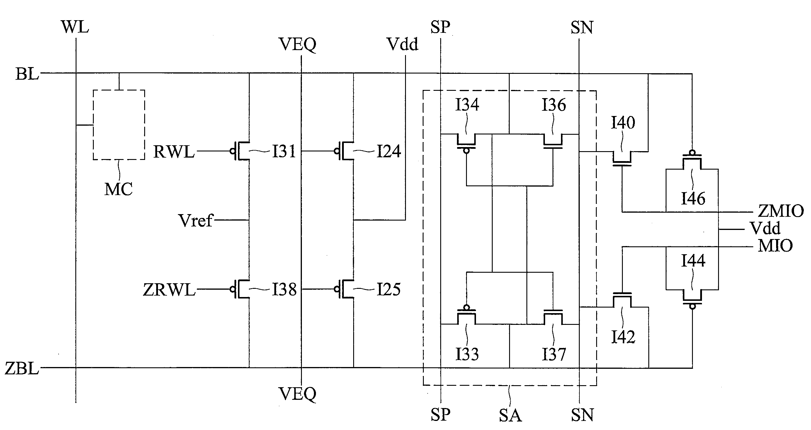
[0041]FIG. 3 depicts a full Vdd level sense amplifier SA and a global and local bit line arrangement implementing a first preferred circuit embodiment of the invention. In FIG. 3, an example memory cell MC is disposed at an intersection of a word or row line labeled WL and a local bit line BL. Although not shown, many other memory cells are similarly disposed in order to complete the memory array. Complementary bit line ZBL is also shown drawn parallel to bit line BL. Memory cell MC comprises an access transistor (not shown for clarity) having a control input coupled to the w...


PUM


Abstract

A circuit and method for a sense amplifier for sensing the charge stored by a memory cell is disclosed. The memory cell is coupled to a bit line, a complementary bit line and a differential sense amplifier is coupled to the bit line and the complementary bit line. A control signal couples a reference voltage to the complementary bit line. A positive precharge voltage is applied to the bit line and complementary bit line prior to the sense amplifier being enabled. The memory cell outputs a voltage to the bit line responsive to a word line, and the sense amplifier senses the differential voltage between the bit line and the complementary bit line responsive to a sense enable signal. A voltage regulator for generating the reference voltage, preferably about 80% of a positive supply voltage, is disclosed. A method of sensing data stored by a memory cell is disclosed.

Description

TECHNICAL FIELD[0001]The present invention relates to a circuit and method for providing an improved sense amplifier and an associated voltage reference regulator circuit for use in dynamic memory circuits.BACKGROUND[0002]Highly integrated semiconductor circuits are increasingly important, particularly in producing battery-operated devices such as cell phones, portable computers (such as laptops), notebook computers and PDAs, wireless email terminals, MP3 audio and video players, portable wireless web browsers and the like, and these sophisticated integrated circuits increasingly include on-board data storage.[0003]As is known in the art, such data storage may take the form of dynamic memory cells in which arrays of capacitive storage memory cells are provided, each memory cell having an access transistor. Data stored in such memory cells is actually a charge stored on a small capacitor, and the data is typically accessed by outputting the stored charge to a bit line coupled to a se...

Claims


Application Information

Patent Timeline
Patent Type & Authority Applications(United States)
IPC IPC(8): G11C7/08G11C7/12
CPCG11C7/08G11C7/12G11C11/4097G11C11/4094G11C11/4091
Inventor HSU, KUOYUAN PETERKIM, YOUNG SUKWANG, BINGHUANG, MING CHIEH
Owner TAIWAN SEMICON MFG CO LTD
Why Eureka
Try Eureka