Optical Micro-Connector

a micro-connector and optical technology, applied in the field of optical micro-connectors, can solve the problems of limited signal transmission distance, large power consumption, high resistance, etc., and achieve the effects of reliable micro-devices, high speed connections, and low cos

Inactive Publication Date: 2009-09-17
II VI DELAWARE INC
View PDF31 Cites 5 Cited by
  • Summary
  • Abstract
  • Description
  • Claims
  • Application Information

AI Technical Summary

Benefits of technology

[0004]One advantage of the present invention is it permits high speed connections through a single fiber at a very low cost and through a very reliable microdevice. Another advantage of the invention is the capability of the connector in preventing connection failure due to improper seating of an optical fiber while simultaneously exhibiting a small footprint for easy incorporation into most PCB applications.
[0005]Accordingly, the present invention encompasses a method of transferring information between first and second printed circuit boards, said method comprising the conversion of electrical impulses from a first printed circuit board to optical signals, transferring said optical signals from said first circuit board to said second circuit board over a single bare optical fiber connected to both of said printed circuit boards through microconnection devices, and converting said optical signals to electrical impulses at said second circuit board, wherein no silicon waveguides are utilized. Furthermore, encompassed as well within the invention is the same method wherein the rate of information transfer is at least 10 Gb / s over said bare fiber.
[0006]The above-described advantages are achieved by mounting an optical transmitter module or an optical receiver module directly onto a PCB (printed circuit board) with silicon circuitry near or underneath the module. The transmitting or receiving modules execute spatial optical transmission of signals converted from electrical impulses to optical signals by the silicon circuitry to which they are attached. This signals are then transmitted between the optical transmitting module and the optical receiving module via an optical fiber held in position by the current micro-connector invention.
[0007]More specifically, in one embodiment of the present invention, there is provided an optical connector for connecting electronic components co-located on the same PCB or on separate PCBs and having a first connector and second connector for transmitting and receiving information between such components. The first connector includes at least an optical transmitter that converts electric signal input to an optical signal output and transmits said data via an optical fiber to a second connector. The second connector includes at least one optical receiver module that converts optical signal input from the optical transmitter module of the first connector and outputs electrical signal output to be used by components on the PCB.
[0008]One potentially preferred embodiment of the invention can provide an optical connector in which costly silicon waveguides are not utilized. Further, high-speed and high-capacity transmitting can be achieved on PCBs by adopting optical transmission as a means of transmitting data between components.
[0009]In a second potentially preferred embodiment, there is provided an optical connector for connecting electronic components co-located on the same PCB or on separate PCBs and having a first connector and second connector for transmitting information between such components. The first connector includes at least an optical transmitter that converts electric signal input to an optical signal output and transmits data via an optical fiber to a second connector. The second connector includes at least one optical receiver module that converts optical signal input from the optical transmitter module of the first connector and outputs electrical signal output to be used by components on the PCB. The second connector may also include at least one optical transmitter to convert electrical signal input to an optical signal output and transmit the output via the same optical fiber back to the first connector which then includes at least one optical receiver module that converts optical signal input from the optical transmitter module of the second connector and outputs electrical signal output to be used by components on the PCB.

Problems solved by technology

As processing speeds increase, however, the skin effect of high frequency signals can create a host of problems including high resistance, large power consumption, and limited signal transmission distance.
While optical connections have always been known for their speed and reliability they have also been associated with a high cost of implementation.
However, until now there has been a lack of adequate small form-factor and low cost micro-connectors for utilization in optical interconnections.

Method used


Image

  • Optical Micro-Connector
  • Optical Micro-Connector
  • Optical Micro-Connector

Examples


Embodiment Construction

[0020]Detailed embodiments of the present invention are disclosed herein; however, as will be readily apparent to those skilled in the art, the present invention may be produced in other specific forms without departing from its spirit or essential characteristics. The present embodiments, are therefore, to be considered as illustrative and not restrictive, the scope of the invention being indicated by the claims rather than the following description, and all changes which come within the meaning and range of the equivalence of the claims are therefore intended to be embraced therein.

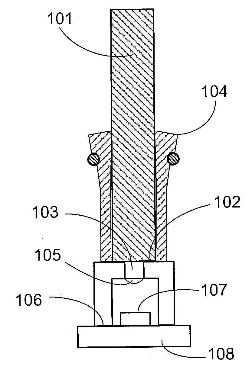
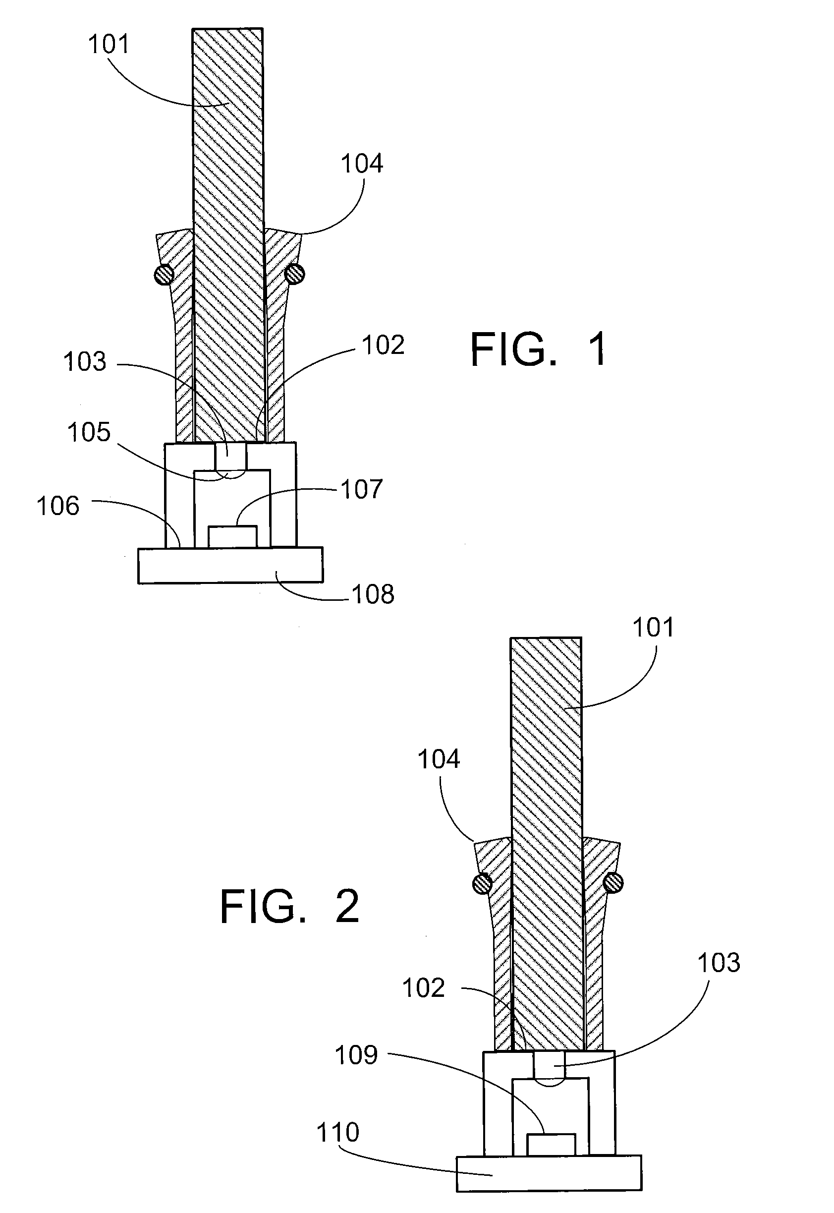
[0021]Referring to FIG. 1, a first connector includes a transmitter 107 which is used to communicate an optical signal to a optical fiber 101. The transmitter 107 can comprise a light source such as a VCSEL and a lens 105, if needed, but it will be understood to those skilled in the art, in view of the disclosure herein, that the transmitter 107 can include a wide variety of devices in any number of con...


PUM


Abstract

A low-cost, high-speed micro-connector replacement for current electrical inter-connects and intra-connects on printed circuit boards is provided. The invention permits fast and reliable information transmission over a single fiber through the utilization of an optical transmitter module or optical receiver module mounted in close proximity to a modulator used to encode optical signals from electrical impulses or decode optical signals to electrical impulses. The micro-connector is mounted on a PCB in alignment with the transmitting or receiving modules and provides appropriate alignment and stop positioning of an optical fiber used for optical transmitting between transmitting/receiving modules.

Description

FIELD OF THE INVENTION[0001]The present invention relates to an optical connector, more particularly to a micro-connector that holds an optical fiber over a laser or detector in order to transmit information by optical means. The invention permits fast and reliable information transmission over a single fiber through the utilization of an optical transmitter module or optical receiver module mounted in close proximity to a modulator used to encode optical signals from electrical impulses or decode optical signals to electrical impulses. The micro-connector is mounted on a PCB in alignment with the transmitting or receiving modules and provides appropriate alignment and stop positioning of an optical fiber used for optical transmitting between transmitting / receiving modules.BACKGROUND OF THE INVENTION[0002]As future high speed computing technologies find a need to transfer large amounts of data from point to point between electronic components, technologies will have to adapt in orde...

Claims


Application Information

Patent Timeline
Patent Type & Authority Applications(United States)
IPC IPC(8): H04B10/00
CPCG02B6/4292G02B6/3809
Inventor DENG, HONGYU
Owner II VI DELAWARE INC
Why Eureka
Try Eureka