Stage and electron microscope apparatus

a stage mechanism and electron microscope technology, applied in electrical apparatus, electrical discharge tubes, nuclear engineering, etc., can solve the problems of deteriorating electrical resistance against external noise, complicated circuits, and deteriorating measurement accuracy, and achieve the effect of small dri

Inactive Publication Date: 2009-09-24
HITACHI HIGH-TECH CORP
View PDF7 Cites 12 Cited by
  • Summary
  • Abstract
  • Description
  • Claims
  • Application Information

AI Technical Summary

Benefits of technology

[0018]According to the embodiment of the invention, it may be possible to achieve a sample stage that has small drift when stopped, and an electron microscope using the sample stage.

Problems solved by technology

Meanwhile, if drift occurs on a sample stage, that is, if the stop position of the sample is minutely deviated with time after the sample is completely positioned while the sample is observed with high magnification, there is a problem in that measurement accuracy deteriorates during the measurement of the dimensions of fine patterns.
As a result, there are problems in that the circuit is complicated and that the electrical resistance against external noise deteriorates.
Accordingly, if the ultrasonic motor and the stage using the ultrasonic motor are used in the electron microscope for inspecting and measuring a semiconductor, there is a problem in that it is difficult to reduce drift.
An ultrasonic motor using a piezo electric actuator has residual deformation of the piezo electric actuator as a peculiar problem.
However, drift causes a serious problem in the electron microscope for inspecting and measuring a semiconductor where a permissible value of drift is strict as described above.

Method used


Image

  • Stage and electron microscope apparatus
  • Stage and electron microscope apparatus
  • Stage and electron microscope apparatus

Examples


example 1

Application and Apparatus

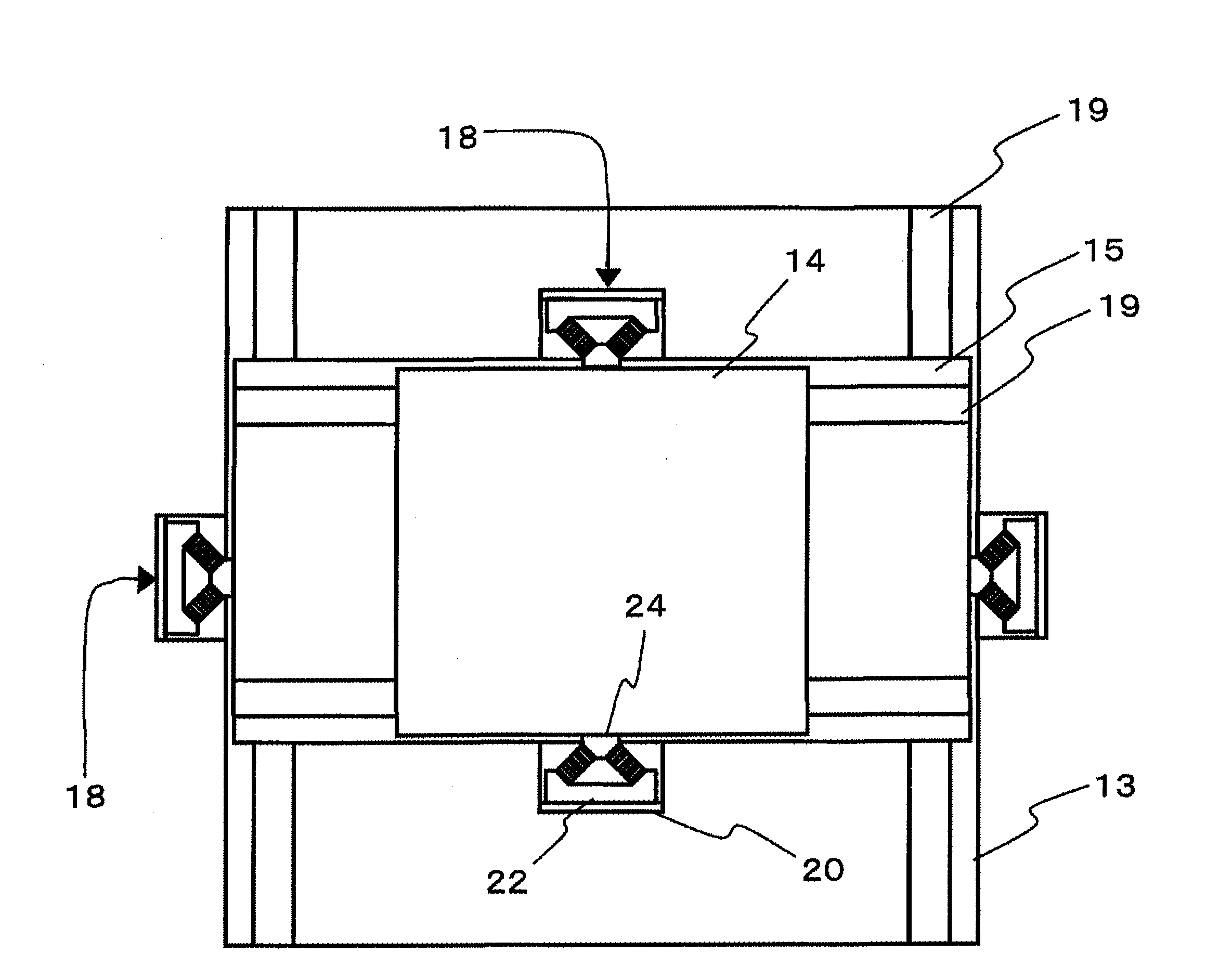
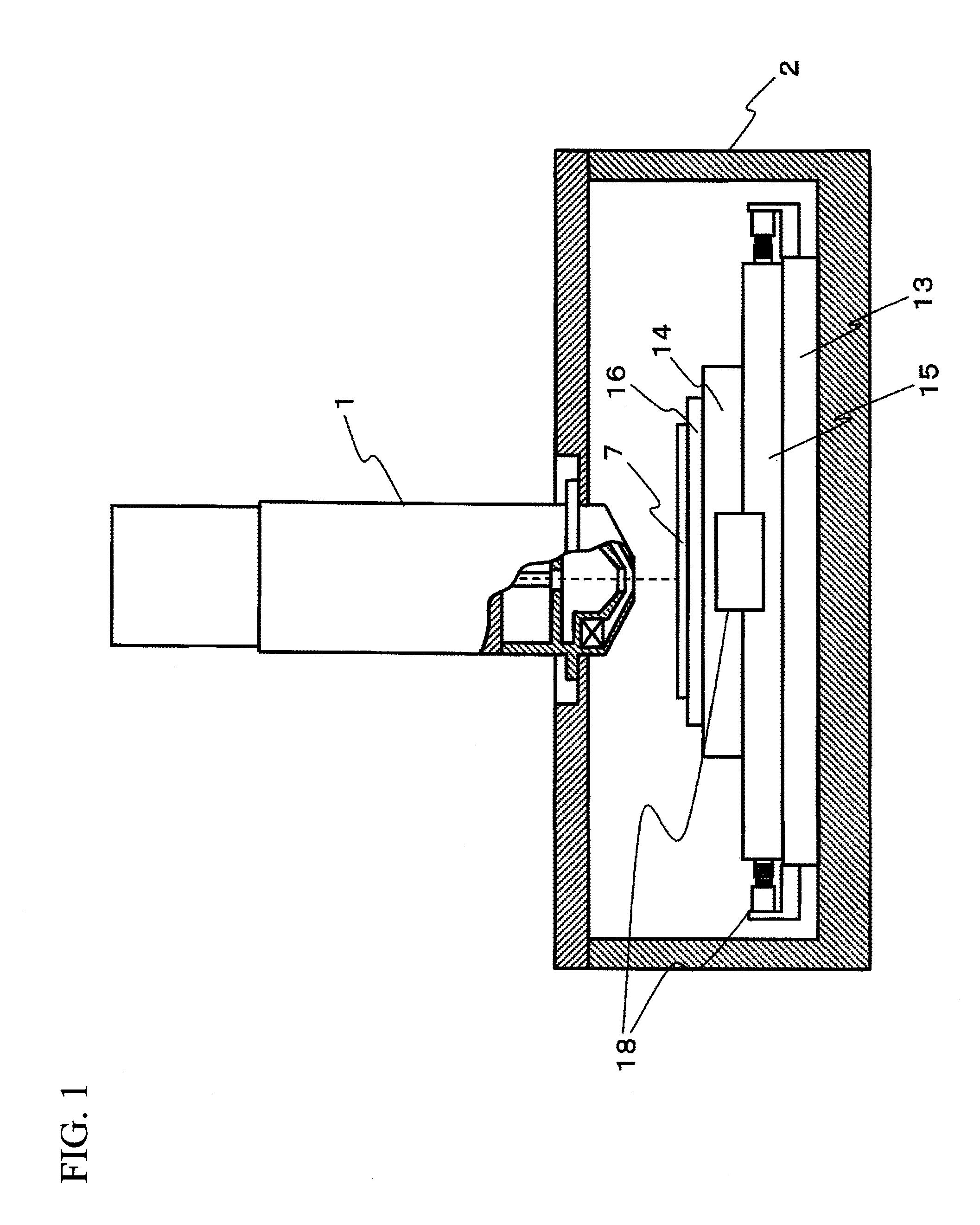
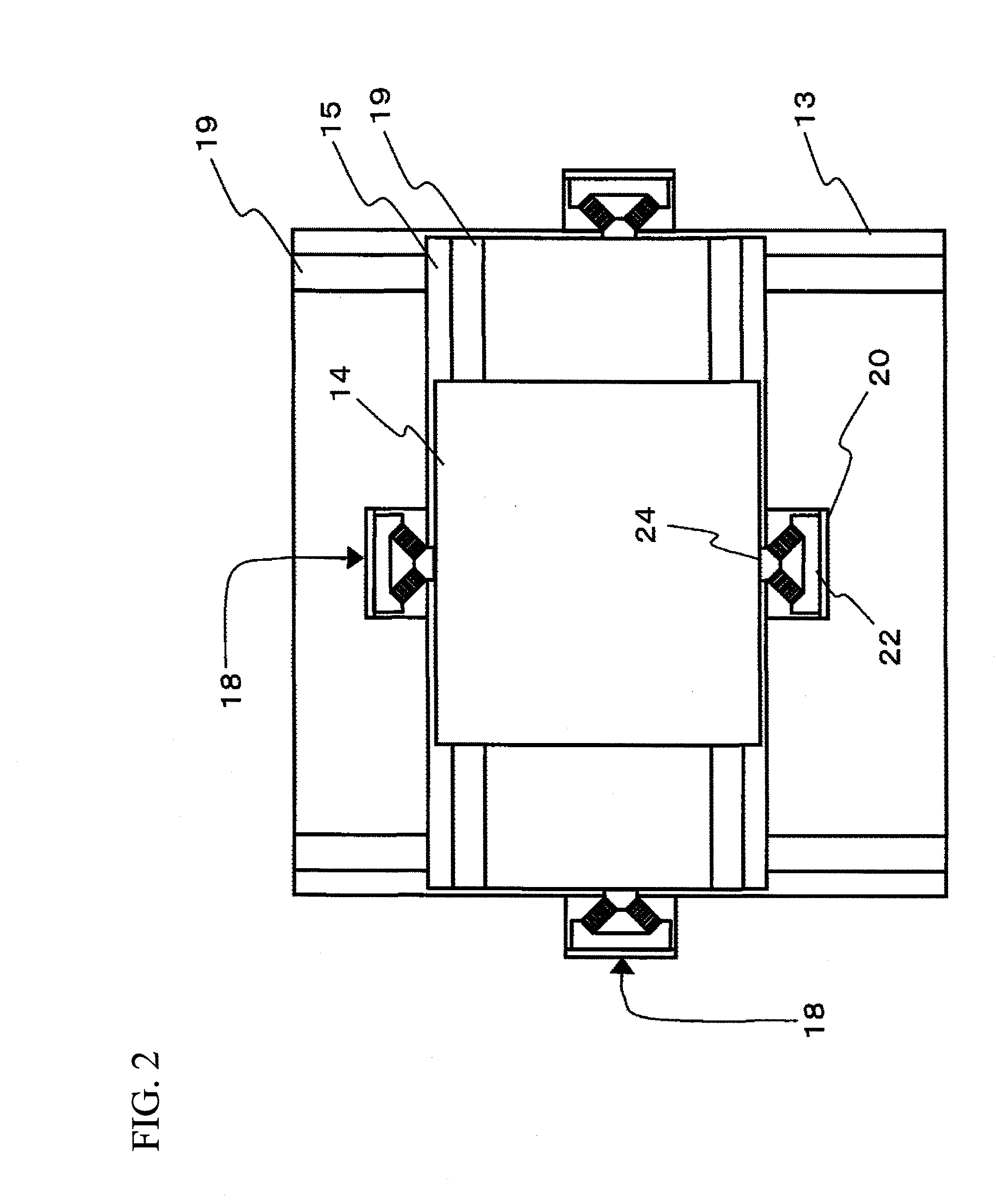
[0044]FIG. 1 is a schematic view showing the configuration of a length measuring SEM according to an embodiment of the invention. The length measuring SEM according to the embodiment of the invention includes a charged-particle optical system 1, a sample chamber 2 that keeps a wafer (sample) 7 in a vacuum, and a sample stage that moves the wafer 7. The length measuring SEM scans the wafer 7 with a charged particle beam that is emitted from the charged-particle source and thinly focused on the wafer, obtains a scanned image of the wafer 7 by detecting secondary electrons that are emitted from the wafer 7, and measures the dimensions of fine patterns formed on the wafer from signals of the scanned image.

[0045]The sample chamber 2 is kept in a vacuum state, which corresponds to a vacuum pressure of about 10−4 Pa, by a vacuum pump (not shown) or the like. The sample stage disposed in the sample chamber 2 is a mechanism that moves and positions an arbitrary porti...

example 2

Set Phase Cutoff

[0058]Another method of reducing the drift of the table in the same apparatus as Example 1 will be described with reference to FIGS. 9 and 10. Positioning accuracy has deteriorated due to the residual friction force in Example 1. However, since the positioning accuracy significantly deteriorates if the residual friction force is large, this is not necessarily preferable. Accordingly, a method of reducing drift by controlling the phase of drive cutoff without the deterioration of the positioning accuracy is used in this example.

[0059]FIG. 9 shows a method of controlling the residual deformation by using a cutoff phase in the same graph (a graph showing a relationship between deformation and the voltage applied to the piezo electric actuator) as FIG. 8. Oblique dotted lines in FIG. 9 are tangent lines that are tangent to the deformation characteristic graph and parallel to the deformation convergence line. In order to prevent the positioning accuracy from deteriorating...

example 3

Serial Motor

[0065]This example provides a method of reducing drift when a serially disposed ultrasonic motor is used unlike in Examples 1 and 2. FIGS. 12A and 12B are views showing a structural example and modification of the serially disposed ultrasonic motor. The ultrasonic motor 18 includes an expandable piezo electric actuator 23A, a shearing piezo electric actuator 23B, and a drive tip 24 that are stacked on a pedestal 22. Like the ultrasonic motor of the above-mentioned example, the trajectory of the drive tip 24 may be controlled by a phase difference between the applied voltages that are applied to the piezo electric actuators. As shown in 12A and 12B, the expandable piezo electric actuator 23A operates to press the drive tip 24 against the drive face, and the hearing piezo electric actuator 23B sliding in the moving direction of the stage operates to move the stage in the moving direction of the stage. The sample stage is moved in a predetermined direction by the cooperatio...


PUM


Abstract

A sample stage for electron microscope according to an embodiment of the invention includes at least two actuators capable of expanding and contracting or capable of swinging for moving a target sample in a predetermined direction. With a coordination of the two actuators, various controls are available by combining the operations of the two actuators. Accordingly, a stage mechanism capable of reducing a stop drift as well as moving a stage can be provided.

Description

BACKGROUND OF THE INVENTION[0001]1. Field of the Invention[0002]The present invention relates to an electron microscope and a stage mechanism for an electron microscope, and more particularly, to an electron microscope that are suitable for measuring dimensions of fine patterns of a semiconductor device or observing the fine patterns and a stage mechanism for the electron microscope.[0003]2. Background Art[0004]A scanning electron microscope (SEM) is used in various fields of research and development, and has been applied in a manufacturing field in recent years. In particular, the measurement of dimensions of fine structure or observation of the fine structure, which is performed by a scanning electron microscope, becomes necessary in a process for manufacturing a semiconductor.[0005]The design rule of a semiconductor integrated circuit becomes finer every year, then the width of a pattern reaches 100 nm or less. Accordingly, a length measuring SEM or a review SEM is used to measur...

Claims


Application Information

Patent Timeline
Patent Type & Authority Applications(United States)
IPC IPC(8): H01J37/20
CPCH01J37/20H01J37/265H01J2237/20264H01J2237/0216H01J37/28
Inventor SEYA, EIICHINAGAMATSU, TAKASHI
Owner HITACHI HIGH-TECH CORP
Why Eureka
Try Eureka