
SRAM Devices Utilizing Strained-Channel Transistors and Methods of Manufacture

Active Publication Date: 2009-09-24
TAIWAN SEMICON MFG CO LTD
View PDF9 Cites 45 Cited by
  • Summary
  • Abstract
  • Description
  • Claims
  • Application Information

AI Technical Summary

Benefits of technology

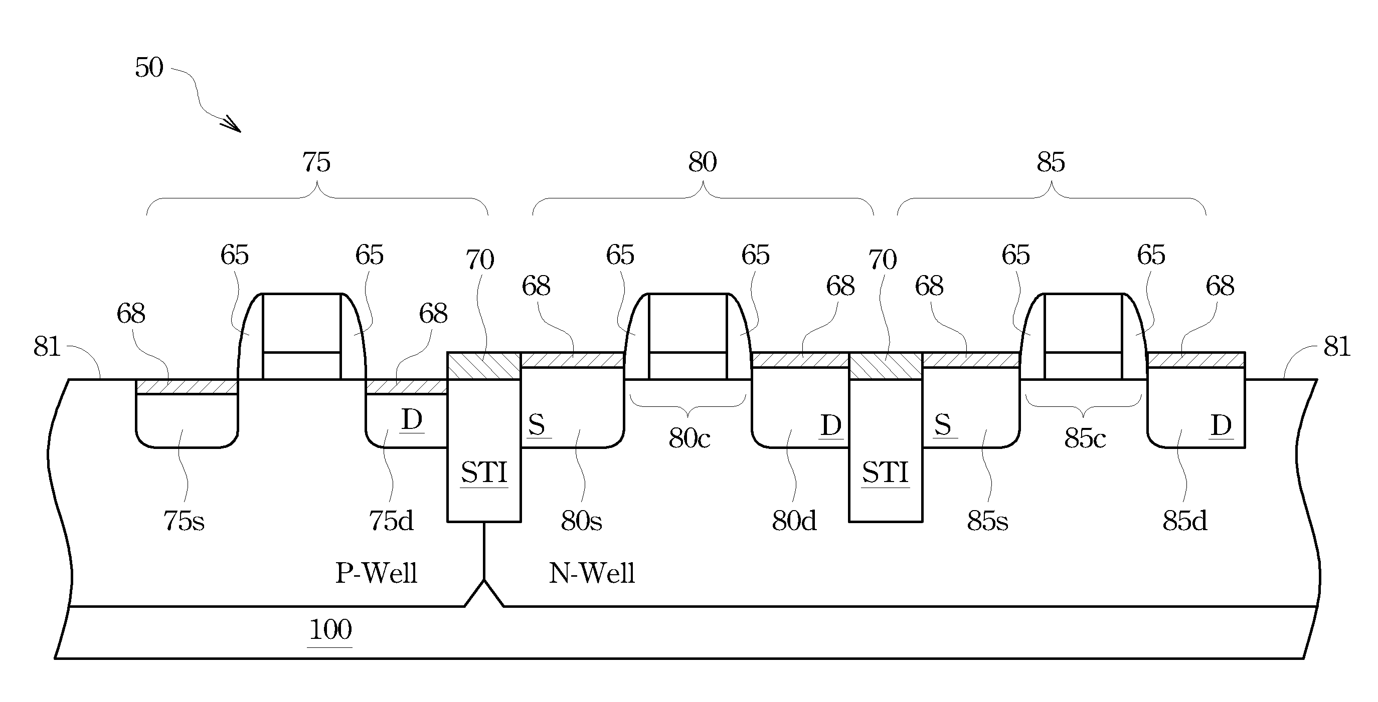
[0007]These and other problems are generally solved or circumvented, and technical advantages are generally achieved, by preferred embodiments of the present invention which provides a semiconductor device comprising an insulating layer disposed on an STI that isolates adjacent MOS devices. The insulation layer is substantially elevated from the semiconductor substrate surface. The elevated insulation layer facilitates the formation of desirable thick epitaxial source / drain regions, and prevents the lateral extension of the source / drain epitaxial layers. The inventive device structure may lead to improved MOS transistor performance, improved SRAM memory cell performance, and improved overall SRAM product manufacturing yield.

Problems solved by technology

This situation may slow down the pace of continuously scaling-down device feature sizes and increasing memory cell density in an SRAM.
This problem prevents forming thick SiGe epitaxial layer that typically provides favorable electrical characteristics, such as reduced contact resistance.
This problem may also lead to reduced SRAM cell manufacturing yield.

Method used


Image

  • SRAM Devices Utilizing Strained-Channel Transistors and Methods of Manufacture
  • SRAM Devices Utilizing Strained-Channel Transistors and Methods of Manufacture
  • SRAM Devices Utilizing Strained-Channel Transistors and Methods of Manufacture

Examples


Embodiment Construction

[0018]The making and using of the presently preferred embodiments are discussed in detail below. It should be appreciated, however, that the present invention provides many applicable inventive concepts that can be embodied in a wide variety of specific contexts. The specific embodiments discussed are merely illustrative of specific ways to make and use the invention, and do not limit the scope of the invention.

[0019]The present invention will be described with respect to preferred embodiments in a specific context, namely improved SRAM devices and SRAM cell structures, and a method of forming the same. This inventive SRAM cell structure comprises an elevated insulation layer on a device isolation region between adjacent PMOS source / drain regions that comprise an elevated epitaxial SiGe layer. The integration of an elevated insulation layer on the device isolation region may be fabricated adding few processing steps that are compatible with a conventional CMOS process flow, for exam...


PUM


Abstract

A novel SRAM memory cell structure and method of making the same are provided. The SRAM memory cell structure comprises strained PMOS transistors formed in a semiconductor substrate. The PMOS transistors comprise epitaxial grown source / drain regions that result in significant PMOS transistor drive current increase. An insulation layer is formed atop an STI that is used to electrically isolate adjacent PMOS transistors. The insulation layer is substantially elevated from the semiconductor substrate surface. The elevated insulation layer facilitates the formation of desirable thick epitaxial source / drain regions, and prevents the bridging between adjacent epitaxial layers due to the epitaxial layer lateral extension during the process of growing epitaxial sour / drain regions. The processing steps of forming the elevated insulation layer are compatible with a conventional CMOS process flow.

Description

TECHNICAL FIELD[0001]The present invention relates generally to semiconductor devices and more particularly to SRAM devices and SRAM cell structures that utilize strained-channel transistors to enhance the performance of transistors and methods of manufacturing the same.BACKGROUND[0002]While the trend of integrating complex electronic systems in an integrated circuit (IC) continues, there is an increasing demand for high-performance memory devices for storing software programs and processed data. As a reliable, proven technology, a Static Random Access Memory (SRAM) is the instinctive choice of a high-performance stand-alone memory device or an embedded memory device used in ICs having a system-on-a-chip (SOC) configuration. The distinct advantages of an SRAM include fast access speed, low power consumption, high noise margin, and process compatibility with a conventional CMOS fabrication process, among others. There is a continuous quest for SRAMs with higher storage cell density s...

Claims


Application Information

Patent Timeline
IPC IPC(8): H01L27/092
CPCH01L27/11H01L21/823864H01L21/8238H01L27/1104H10B10/00H10B10/12
Inventor CHUANG, HARRYTSAI, HUNG-CHIHTHEI, KONG-BENGLIANG, MONG-SONG
Owner TAIWAN SEMICON MFG CO LTD
Learn More