

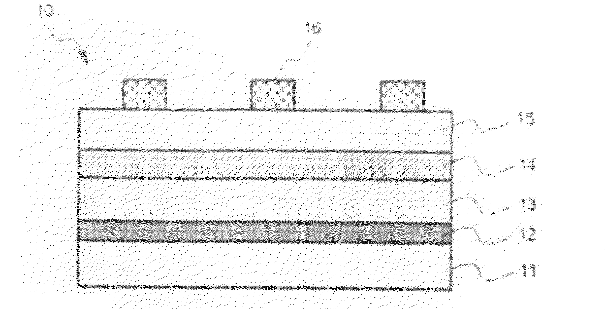
Method For Preparing Cis Compounds and Thin Layer, and Solar Cell Having Cis Compound Thin Layer
a technology of cis compounds and thin layers, applied in the field of preparing cis compounds, can solve the problems of cis compound preparing methods using precursor particles that do not show excellent dispersion, coupling and reaction uniformity among precursor particles, and selenium loss, etc., to prevent selenium loss, improve reaction uniformity, and improve efficiency
- Summary
- Abstract
- Description
- Claims
- Application Information
AI Technical Summary
Benefits of technology
Problems solved by technology
Method used
Image

Examples
example 1
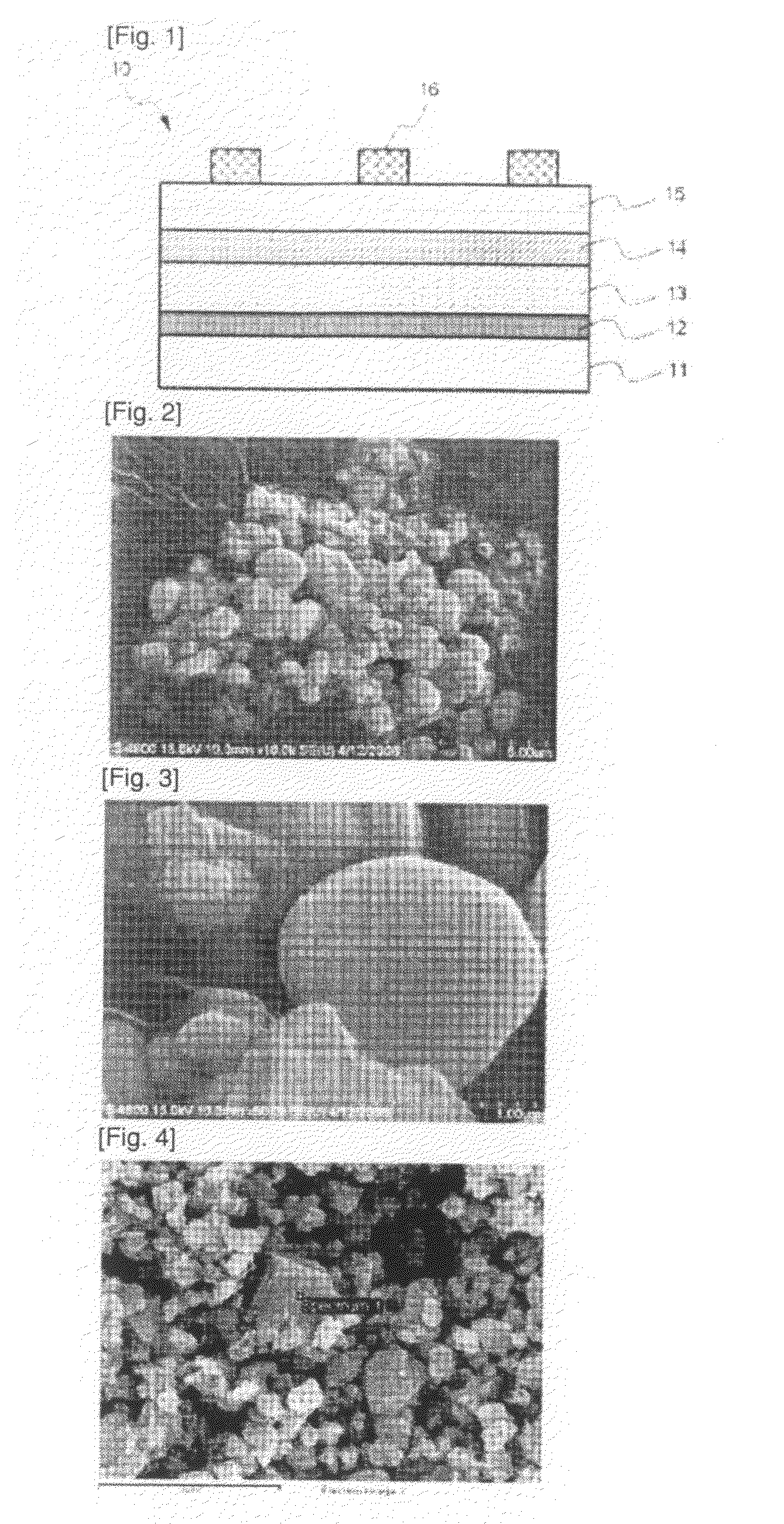
[0067]2 g of In—Se particles were mixed as seed particles in 250 ml of a diethylene glycol solvent together with 2 g of copper nitrate and 2 g of selenous acid as reactant precursors. The reaction solution was heated to 170° C. and reacted for about 3 hours to produce composite particles. SEM (Scanning Electronic Microscope) photographs for the composite particles are respectively shown in FIGS. 2 and 3 (FIG. 2: 10,000 magnifications, FIG. 3: 50,000 magnifications). The photographs of FIGS. 2 and 3 are respectively obtained at an acceleration voltage of 15 keV using a JSM-6340F electronic microscope manufactured by JEOL. As shown in these photographs, it would be found that the composite particle is obtained in a core-cell structure where copper selenide is coated on an indium selenide particle.
[0068]Powder of the product mixture was mixed with terpineol as a solvent and polypropylene carbonate as a binder, and then made into paste. The paste was coated on a substrate, and then RTA ...
example 2
[0071]The experiment identical to the embodiment 1 was repeated, except that 2 g of CuSe particles were mixed as seed particles in 250 ml of a 1,4 butanediol solvent together with 3 g of indium nitrate and 0.06 M of selenous acid as reactant precursors, and the reaction solution was heated to 150° C. and reacted for about 3 hours to produce composite particles.
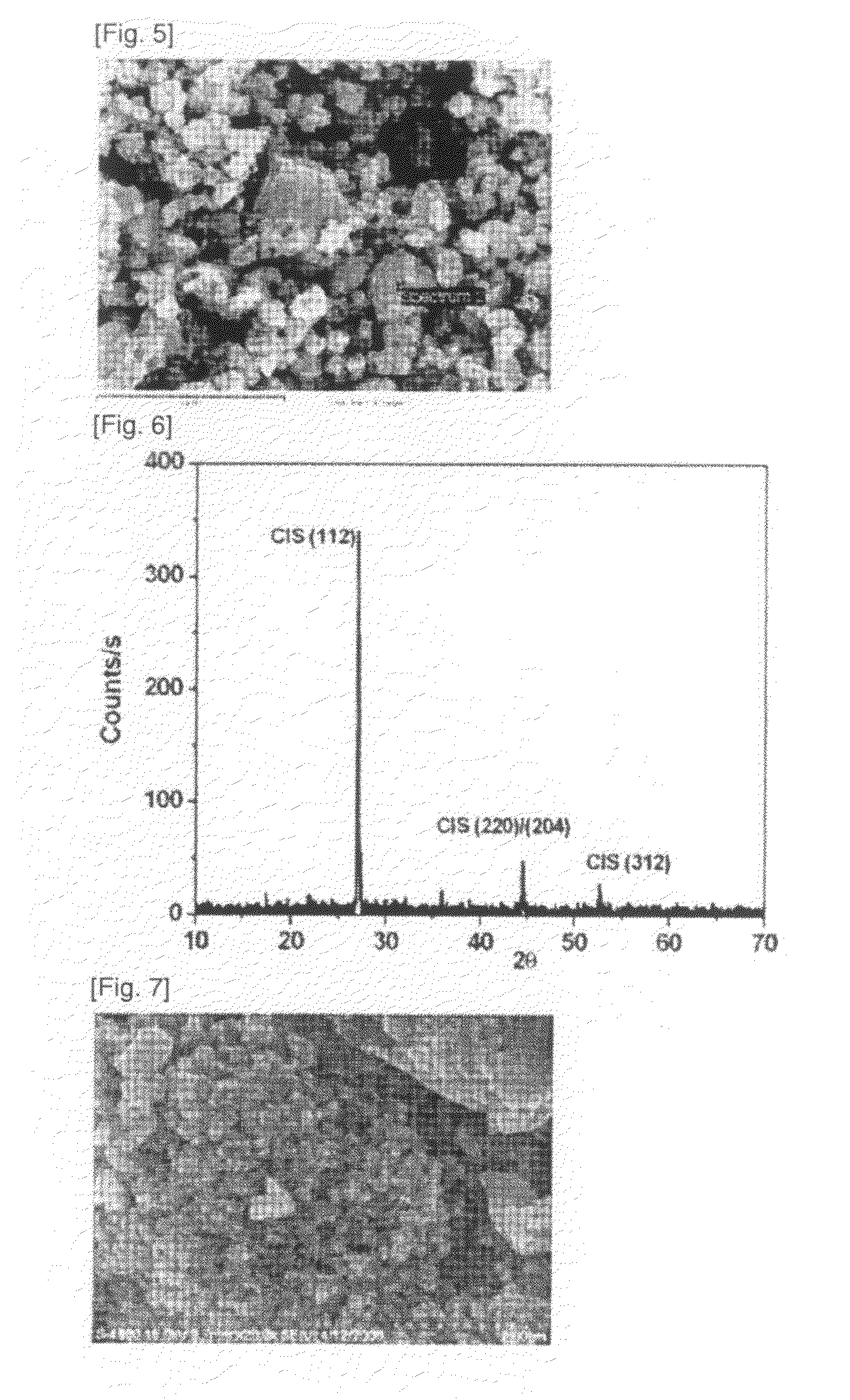
[0072]SEM photographs for the generated composite particles are respectively shown in FIGS. 7 and 8 (FIG. 7: 20,000 magnifications, FIG. 8: 50,000 magnifications). As shown in these photographs, it would be found that the composite particle is obtained in an irregular shape where indium selenide is coated on a copper selenide particle.
[0073]In addition, SEM photographs for the CIS crystal after RTA are respectively shown in FIGS. 9 and 10. As seen from the photographs, it would be found that the crystal finally obtained changes its shape to some level during RTA in comparison to the composite particle of FIGS. 7 and 8.
[0074]In...
PUM
| Property | Measurement | Unit |
|---|---|---|
| size | aaaaa | aaaaa |
| size | aaaaa | aaaaa |
| thickness | aaaaa | aaaaa |
Abstract
Description
Claims
Application Information