Multi-layer wiring board and method of manufacturing the same

a wiring board and multi-layer technology, applied in the direction of sustainable manufacturing/processing, electrical apparatus construction details, final product manufacturing, etc., can solve the problems of difficult to directly connect the ic chip to the mother board, difficult to improve the process speed, and difficult to ensure the strength of the coreless wiring board, etc., to achieve high workability, easy to form the opening of the reinforcing plate, and sufficient adhesion strength

Inactive Publication Date: 2009-10-01
NGK SPARK PLUG CO LTD
View PDF7 Cites 37 Cited by
  • Summary
  • Abstract
  • Description
  • Claims
  • Application Information

AI Technical Summary

Benefits of technology

[0027]According to the above method, since the reinforcing plate made of a non-metal material is fixed to the solder resist in a surface contact state, it is possible to obtain sufficient adhesion strength, as compared to the related art in which a metal reinforcing plate is fixed to the upper surface of a resin insulating layer having a conductor pattern formed thereon. In addition, since the reinforcing plate in step (d) is made of a non-metal material, it has high workability. Therefore, it is possible to easily form the reinforcing plate openings at positions corresponding to the second terminals, and it is also possible to reduce a material cost. Further, since the diameter of the reinforcing plate openings and the diameter of the solder resist openings are set to be smaller than that of the adhesive layer openings, it is possible to firmly fix the reinforcing plate without the adhesive layer protruding toward the inside of the solder resist opening or the inside of the reinforcing plate opening. Therefore, when the solder bumps are provided on the second terminals and the multi-layer wiring board is mounted on another substrate through the solder bumps, it is possible to prevent the melted solder bumps from being contacted with the adhesive layer. As a result, it is possible to prevent an adhesive from being mixed with the solder bumps.
[0028]When the solder bumps or the terminal pins are provided on the second terminals, a step of providing the solder bumps or the terminal pins may be performed before the reinforcing plate adhering step. When the step of providing the solder bumps or the terminal pins is performed after the reinforcing plate adhering step, the thermal stress of soldering in the step of providing the solder bumps or the terminal pins is applied to the reinforcing plate or the adhesive layer. In contrast, when the step of providing the solder bumps or the terminal pins is performed before the reinforcing plate adhering step, it is possible to prevent the thermal stress of soldering from being applied. In addition, when the reinforcing plate or the adhesive layer is made of a material having high heat resistance, the step of providing the solder bumps or the terminal pins may be performed after the reinforcing plate adhering step.
[0029]The adhesive layer is temporarily adhered to one surface of the reinforcing plate in step (d), and then adhered to the solder resist in step (e). Inversely, when the adhesive layer is temporarily adhered to the solder resist and then adhered to the reinforcing plate, the solder bumps or the terminal pins on the second terminals make it difficult to temporarily adhere the adhesive layer. In contrast, since uneven portions, such as the solder bumps or the terminal pins, are not provided in the reinforcing plate, it is possible to easily perform the temporary adhesion of the adhesive layer to one surface of the reinforcing plate in step (d). Further, in step (f), the adhesive layer in a non-hardened state is hardened at a temperature that is lower than a solder melting temperature. Therefore, it is possible to prevent the solder bumps on the second terminals or solder bonding portions that bond the terminal pins to the second terminals from being melted.

Problems solved by technology

However, there is a large difference between the pitch between the terminals in the terminal group of the IC chip and the pitch between the terminals in the terminal group of the mother board, and thus it is difficult to directly connect the IC chip to the mother board.
In this case, the wiring lines passing through the core substrate serve as large inductance, and thus the transmission loss of high-frequency signals or the malfunction of a circuit occurs, which makes it difficult to improve the process speed.
Also, since the coreless wiring board is manufactured without a core substrate, it is difficult to sufficiently ensure the strength of the coreless wiring board.
When a general-purpose adhesive having a relatively low material cost, such as an adhesive only for resin that is used to adhere each resin, is used, it is difficult to obtain sufficient bonding strength.
In addition, the metal reinforcing plate has lower workability and higher material costs than a resin plate.
Therefore, it is difficult to obtain sufficient adhesion strength.
Therefore, there is a concern that the adhesive may be melted by heat applied when the solder bumps are formed, flow into the through-holes, and be mixed as impurities with the solder bumps.

Method used


Image

  • Multi-layer wiring board and method of manufacturing the same
  • Multi-layer wiring board and method of manufacturing the same
  • Multi-layer wiring board and method of manufacturing the same

Examples


Embodiment Construction

[0046]Exemplary embodiments of the present invention will be described with reference to the drawings hereinafter.

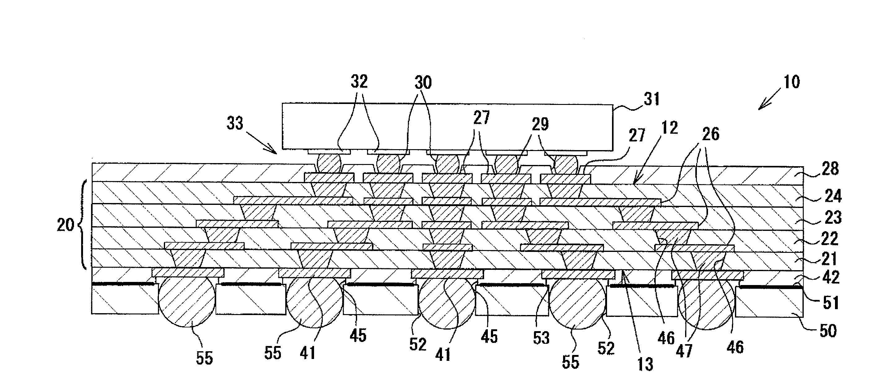
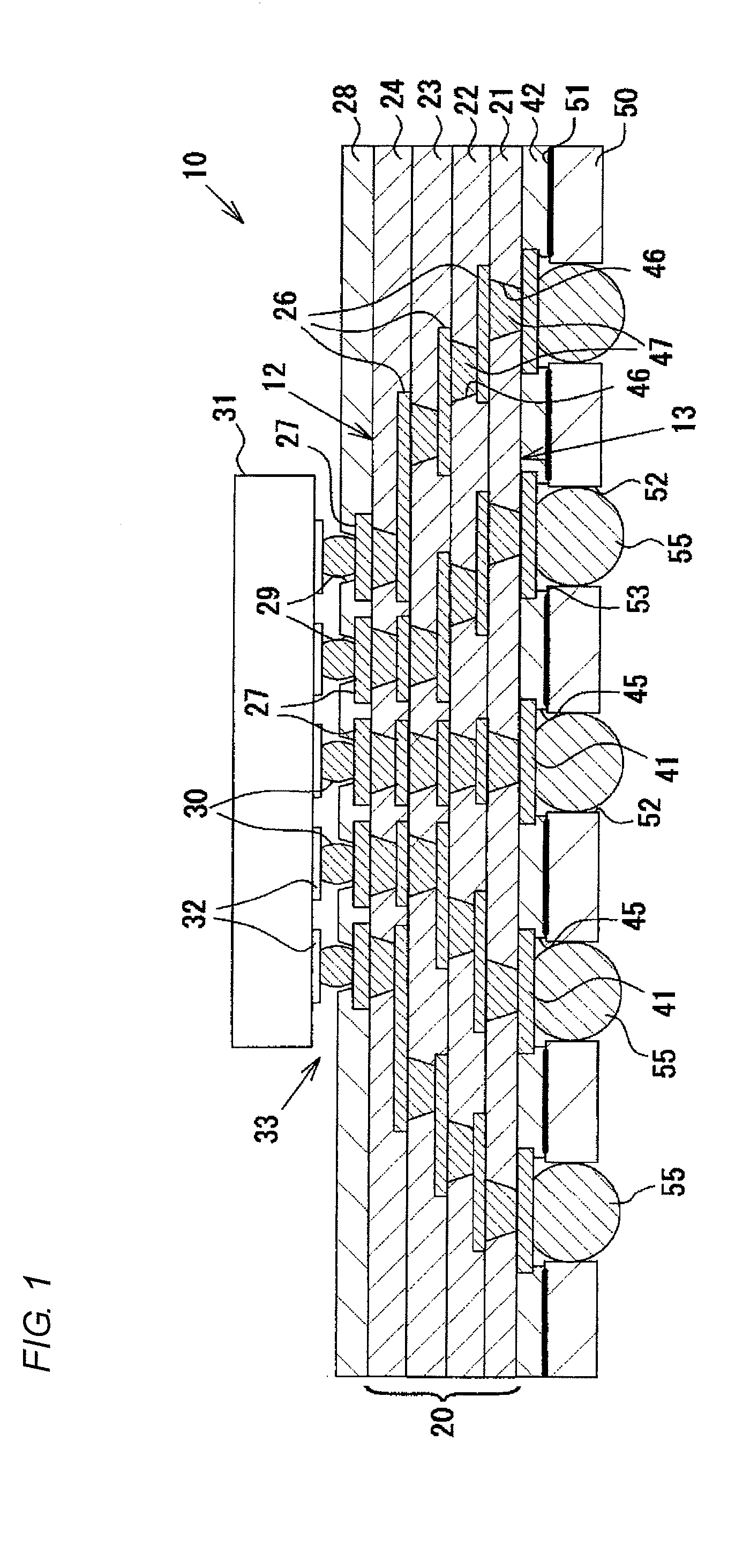
[0047]FIG. 1 is a cross-sectional schematic view illustrating the structure of a coreless wiring board (multi-layer wiring board) according to the exemplary embodiment.

[0048]As shown in FIG. 1, a coreless wiring board 10 does not include a core substrate, and includes a multi-layer laminated structure obtained by alternately forming four resin insulating layers (interlayer insulating layers) 21, 22, 23, and 24 made of epoxy resin and conductor layers 26 made of copper. The resin insulating layers 21 to 24 are interlayer insulating layers that have the same thickness and are made of the same material, and are formed of a sheet-shaped build-up material made of epoxy resin.

[0049]Terminal pads 27 (connection terminals on front surface side) are arranged in an array on a front surface 12 of the coreless wiring board 10 (the front surface of the fourth resin insulating layer 2...


PUM

PropertyMeasurementUnit
diameteraaaaaaaaaa
thicknessaaaaaaaaaa
temperatureaaaaaaaaaa

Abstract

A multi-layer wiring board without a core substrate includes: a multi-layer laminated structure; first terminals provided on a front surface of the multi-layer laminated structure; second terminals provided on a rear surface of the multi-layer laminated structure; a solder resist which covers the rear surface and which has solder resist openings formed at positions corresponding to the second terminals; a reinforcing plate which is made of a non-metal material and which has reinforcing plate openings formed at positions corresponding to the second terminals; and an adhesive layer interposed between the solder resist and the reinforcing plate to fix the reinforcing plate to the solder resist and which includes adhesive layer openings formed at positions corresponding to the second terminals. A diameter of the solder resist openings and a diameter of the reinforcing plate openings are smaller than that of the adhesive layer openings.

Description

CROSS-REFERENCE TO RELATED APPLICATIONS[0001]This application claims priority from Japanese Patent Application No. 2008-086883, filed on Mar. 28, 2008, the entire contents of which are hereby incorporated by reference.BACKGROUND OF THE INVENTION[0002]1. Technical Field[0003]Devices or methods consistent with the present disclosure relate to a multi-layer wiring board that does not include a core substrate.[0004]2. Related Art[0005]In recent years, the process speed of a semiconductor integrated circuit device (IC chip) used as, for example, a microprocessor of a computer has increased, and the functions thereof have been improved. As a result, the number of terminals tends to increase, and the pitch between the terminals tends to be narrowed. In general, a plurality of terminals are densely arranged in an array on the bottom of an IC chip, and the terminal group is connected to terminal group on a mother board by flip-chip bonding. However, there is a large difference between the pi...

Claims


Application Information

Patent Timeline
Patent Type & Authority Applications(United States)
IPC IPC(8): H05K1/03H05K13/00
CPCH01L21/6835Y10T29/49117H01L23/49816H01L23/49822H01L23/49833H01L2221/68345H01L2224/16H01L2924/01078H01L2924/01079H01L2924/15174H01L2924/15311H01L2924/15312H05K3/0064H05K3/025H05K3/303H05K3/3436H05K3/4644H05K2201/10318H05K2201/10424H01L2224/16235H01L23/49811H01L2224/05568H01L2224/05573H01L2924/00014Y02P70/50H01L2224/05599
Inventor ASANO, TOSHIYA
Owner NGK SPARK PLUG CO LTD
Why Eureka
Try Eureka