Non-volatile memory device

a non-volatile memory and device technology, applied in the direction of semiconductor devices, basic electric elements, electrical apparatus, etc., can solve the problems of small variation of oxide thickness, affecting the tunneling of electrons through the bottom oxide, and hardly scaling beyond the 45 nm node of planar nvm devices, so as to reduce the variation of electronic characteristics

Active Publication Date: 2009-10-01
III HLDG 6
View PDF8 Cites 131 Cited by
  • Summary
  • Abstract
  • Description
  • Claims
  • Application Information

AI Technical Summary

Benefits of technology

[0011]It is an object of the present invention to provide a finFET non-volatile

Problems solved by technology

Planar NVM devices, typically based on MOSFET devices, are hardly scaleable beyond the 45 nm node due to short channel effects.
Nevertheless, a small variation of the oxide thickness affects the tunneling of electrons through the bottom oxide significantly.
Clearly, this has undesirable effects on the characteristics of a finFET SONOS memory device, where the bottom oxide is grown after the forma

Method used


Image

  • Non-volatile memory device
  • Non-volatile memory device
  • Non-volatile memory device

Examples


second embodiment

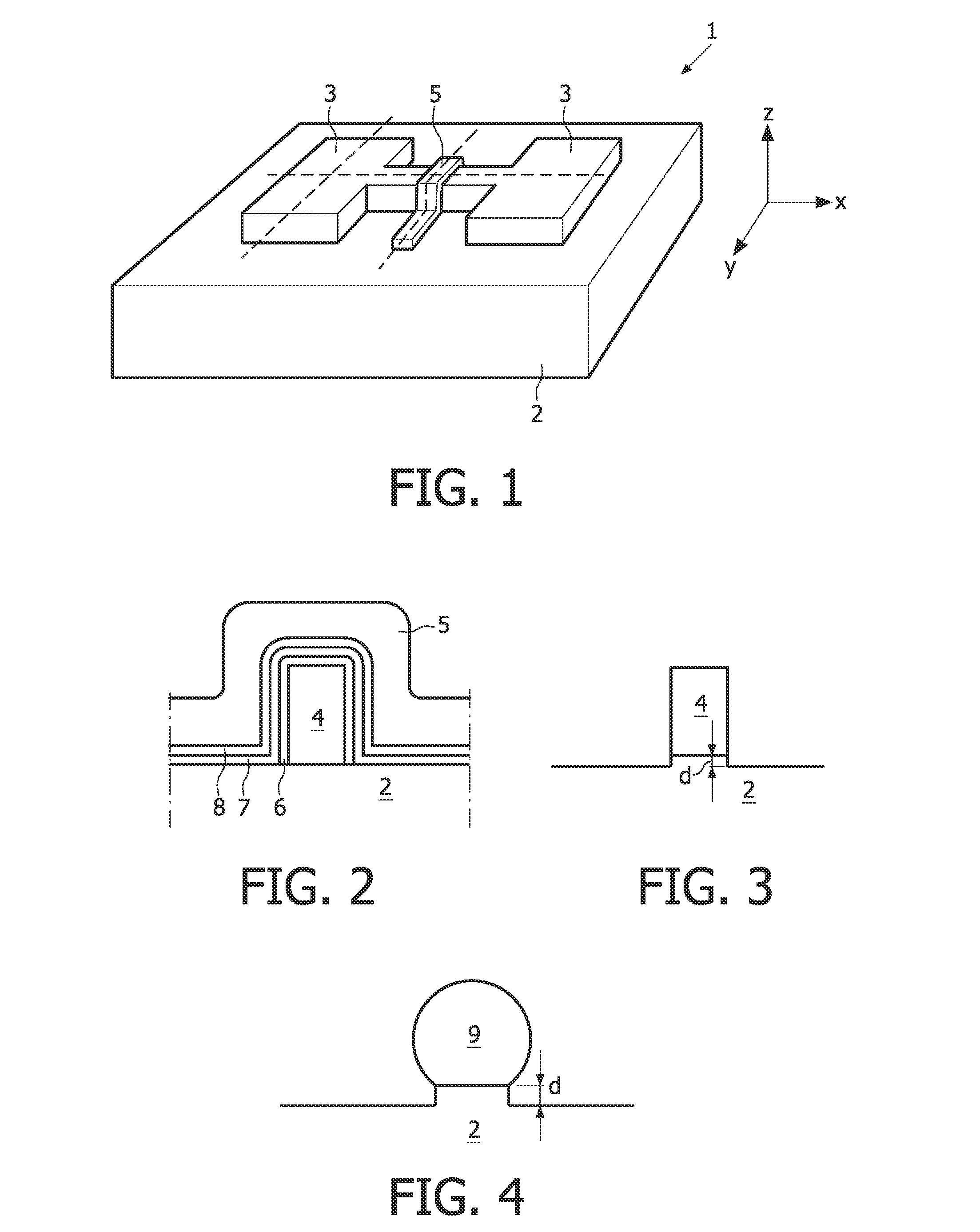
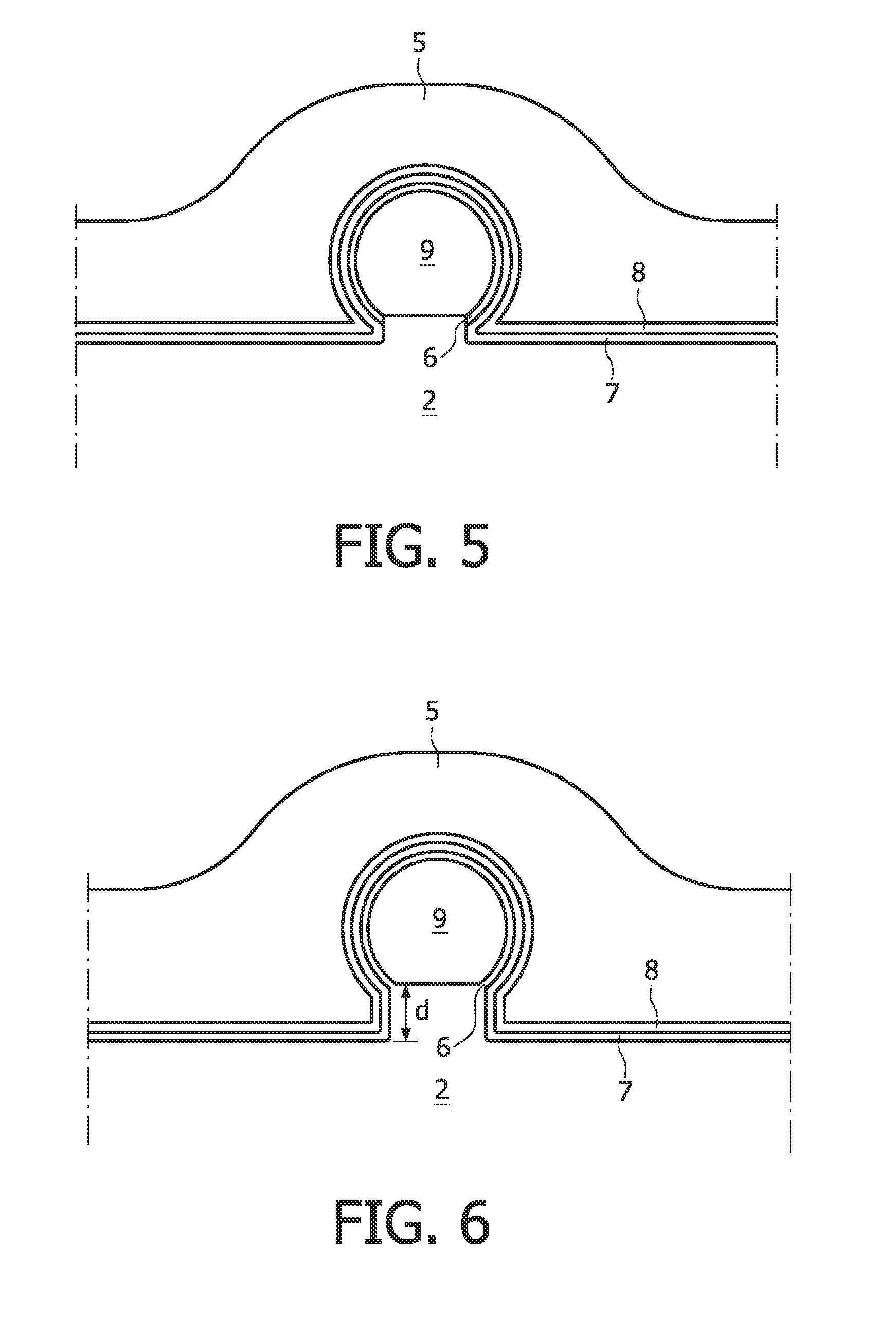
[0089]FIG. 7 shows a cross-sectional view of the finFET-based non-volatile memory device according to the present invention.

[0090]In FIG. 7 entities having the same reference number refer to identical entities as shown in the preceding Figures.

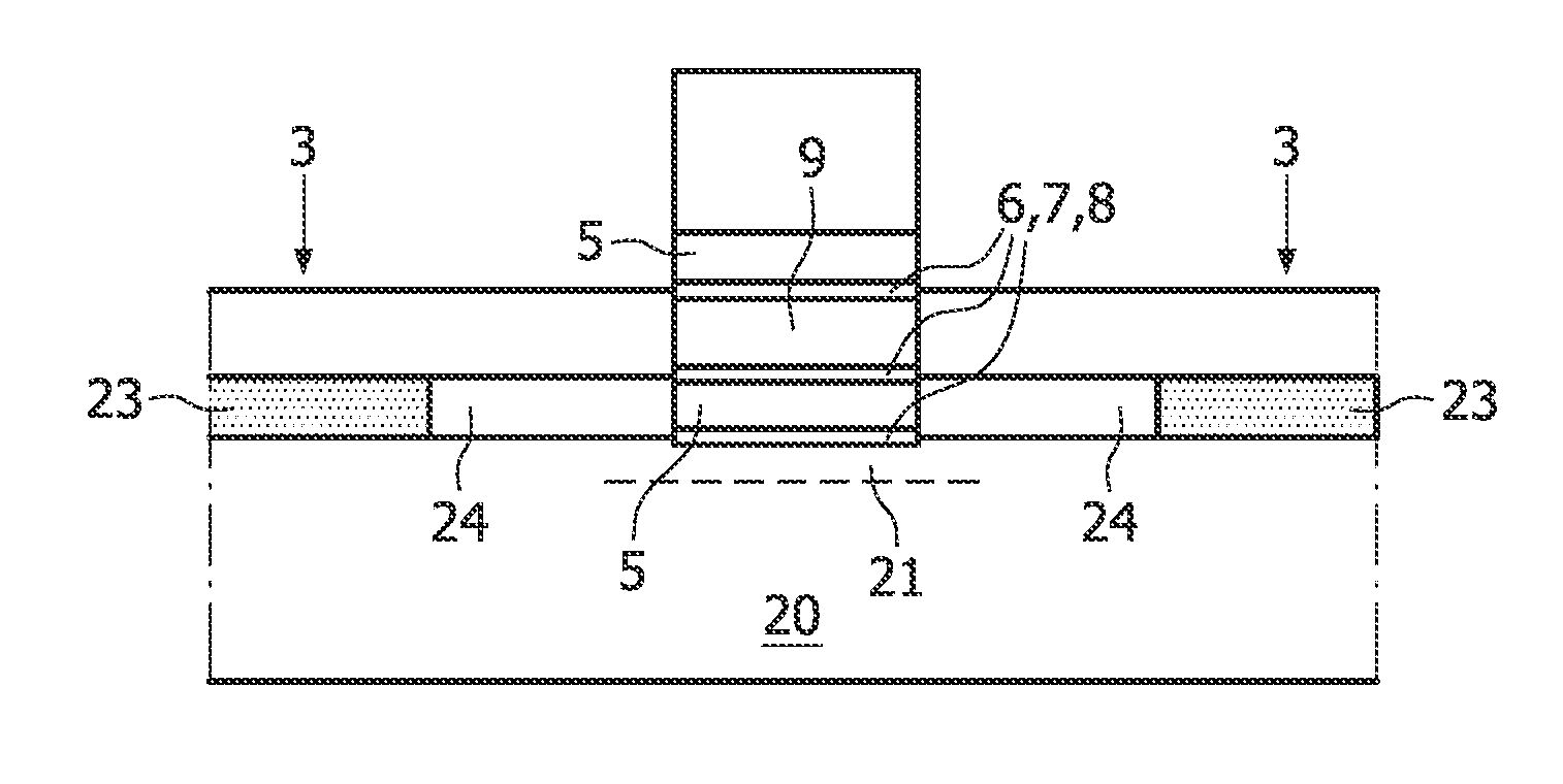
[0091]The cross-section of FIG. 7 is taken along a same line as line A-A, across the gate portion of the finFET-based memory device.

[0092]In this second embodiment, the finFET-based memory device is arranged on a monocrystalline surface layer of an SOI substrate.

[0093]The rounded fin body 9 is free-standing. That is, the circumference of the rounded fin body is not in direct contact with the insulator layer 2. Thus, the rounded fin body 9 can be completely surrounded by the charge trapping stack 6, 7, 8. The full circumference of the rounded fin body 9 is encompassed by the charge trapping stack 6, 7, 8. The charge trapping stack 6, 7, 8, itself is encompassed by the gate 5.

first embodiment

[0094]It is noted that the free hanging fin shown in FIG. 7 can be obtained by largely following the method as discussed above with regard to the Then, when the recess level d is extended (see FIG. 6), the etching is continued to a level where the silicon dioxide under the silicon fin is completely removed, allowing the fin to be free-hanging.

[0095]This extended etching process can be achieved by combining a first step of anisotropic dry etching to partly recess the oxide adjacent to the fin with a second step of isotropic dry etching, which removes the oxide below the fin. Alternatively, the second step may be a wet oxide etching process (e.g. with a HF solution).

third embodiment

[0096]To prevent release of the free hanging Si fin from the substrate, a same construction may be used as is explained below with regard to a finFET-based non-volatile memory device according to a

[0097]According to the first and second embodiments the finFET-based non-volatile memory device is formed on an SOI wafer, while in a third embodiment the finFET-based memory device is formed on a monocrystalline silicon substrate with a buried SiGe layer. Moreover, in accordance with the third embodiment, the fin is free-hanging as shown in FIG. 7. The method of forming the finFET-based non-volatile memory device according to the third embodiment will be illustrated below.

[0098]FIG. 8 shows a second cross-sectional view of the finFET-based non-volatile memory device according to the second embodiment.

[0099]The cross-section of FIG. 8 is taken along a same line as line B-B, across the source / drain region 3, S, D of the finFET-based memory device.

[0100]The source / drain regions 3, S, D are f...


PUM


Abstract

A finFET-based non-volatile memory device on a semiconductor substrate includes source and drain regions, a fin body, a charge trapping stack and a gate. The fin body extends between the source and the drain region as a connection. The charge trapping stack covers a portion of the fin body and the gate covers the charge trapping stack at the location of the fin body. The fin body has a corner-free shape for at least ¾ of the circumference of the fin body which lacks distinct crystal faces and transition zones in between the crystal faces.

Description

FIELD OF THE INVENTION[0001]The present invention relates to a device for non-volatile memory applications. Also, the present invention relates to a method for manufacturing such a device. Moreover, the present invention relates to a memory array comprising such a device for non-volatile memory applications, and also to a semiconductor device comprising such a device for non-volatile memory applications.BACKGROUND OF THE INVENTION[0002]Charge trapping non-volatile memory devices (NVM devices) such as SONOS (silicon dioxide—silicon nitride—silicon dioxide—silicon) and SHINOS (silicon—high K—silicon nitride—silicon dioxide—silicon) memory devices are considered suitable candidates to enable flash memory devices in CMOS generation devices of the 45 nm node and smaller. SONOS and SHINOS memory devices exhibit relatively reduced program and erase voltages. Moreover, these devices are relatively easy to integrate with CMOS logic in case of embedded NVM devices.[0003]Planar NVM devices, ty...

Claims


Application Information

Patent Timeline
IPC IPC(8): H01L29/792H01L21/336H01L21/782
CPCH01L21/28282H01L29/4234H01L29/792H01L29/66833H01L29/66787H01L29/40117
Inventor AKIL, NADERAGARWAL, PRABHATVAN SCHAIJK, ROBERTUS T.F.
Owner III HLDG 6
Why Eureka
Try Eureka