

Plasma processing apparatus, plasma processing method, and computer readable storage medium
- Summary
- Abstract
- Description
- Claims
- Application Information
AI Technical Summary
Benefits of technology
Problems solved by technology
Method used
Image

Examples
first embodiment
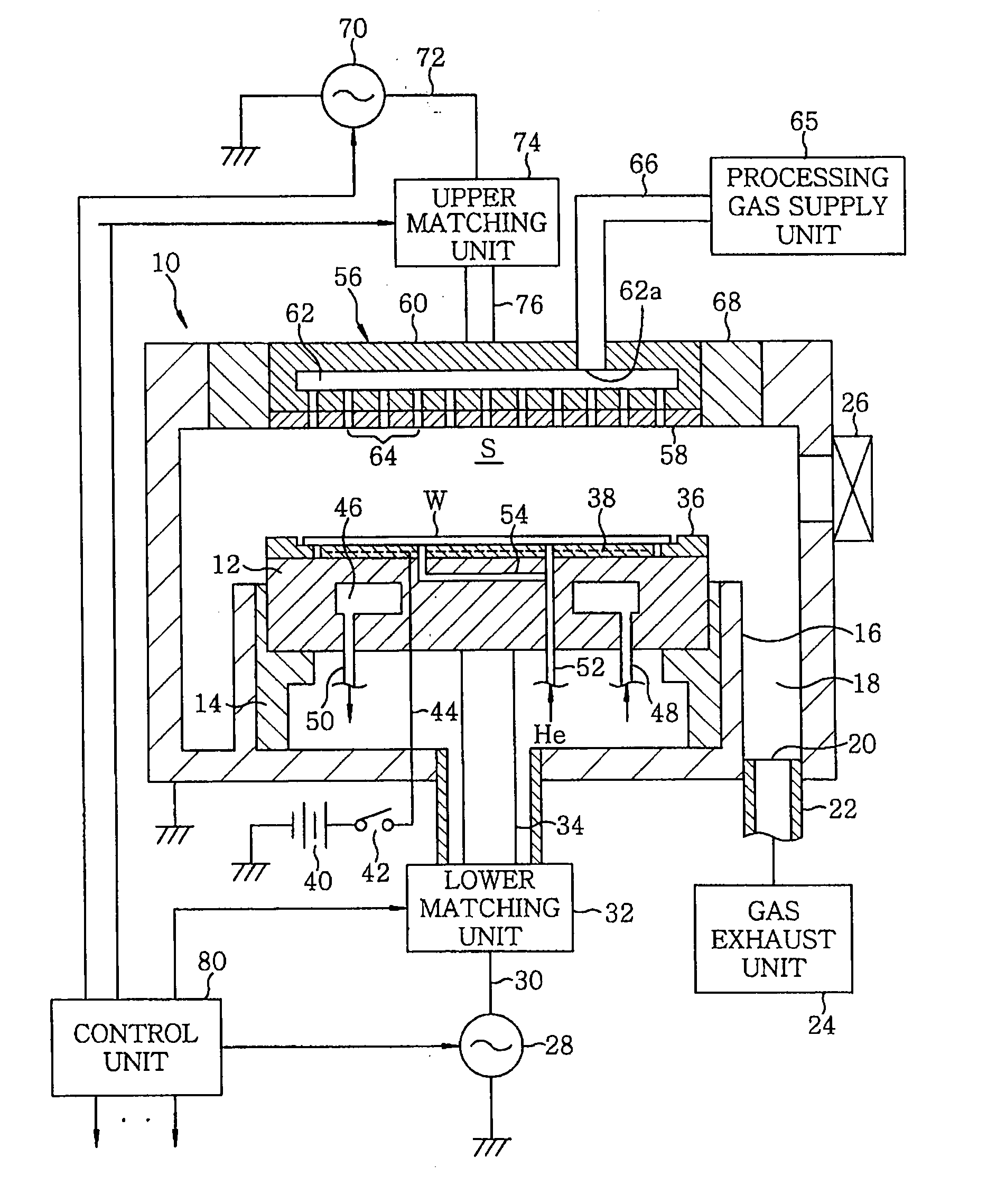
[0064]FIG. 1 shows a configuration of a plasma processing apparatus in accordance with the present invention. This plasma processing apparatus is configured as a capacitively coupled plasma etching apparatus of parallel plates type, and includes a cylindrical chamber (processing vessel) 10 made of metal, e.g., aluminum, stainless steel or the like. The chamber 10 is frame grounded.
[0065]A circular plate-shaped susceptor 12 for mounting thereon a substrate to be processed, e.g., a semiconductor wafer W, is horizontally provided in the chamber 10 and serves as a lower electrode. The susceptor 12 is made of, e.g., aluminum, and is supported, without being grounded, by an insulating cylindrical supporting portion 14 disposed on a bottom of the chamber 10 while extending vertically, the supporting portion 14 being made of, e.g., ceramic. A ring-shaped gas exhaust path 18 is formed along a periphery of the cylindrical supporting portion 14 between a sidewall of the chamber and a conductiv...
third embodiment
[0136]In addition, although it is not illustrated, even in the anode coupled plasma processing apparatus in which the plasma generation radio frequency power HF is supplied to the upper electrode, the HF can be pulse modulated in the manner described in the
[0137]While the invention has been shown and described with respect to the embodiments, it will be understood by those skilled in the art that various changes and modification may be made.
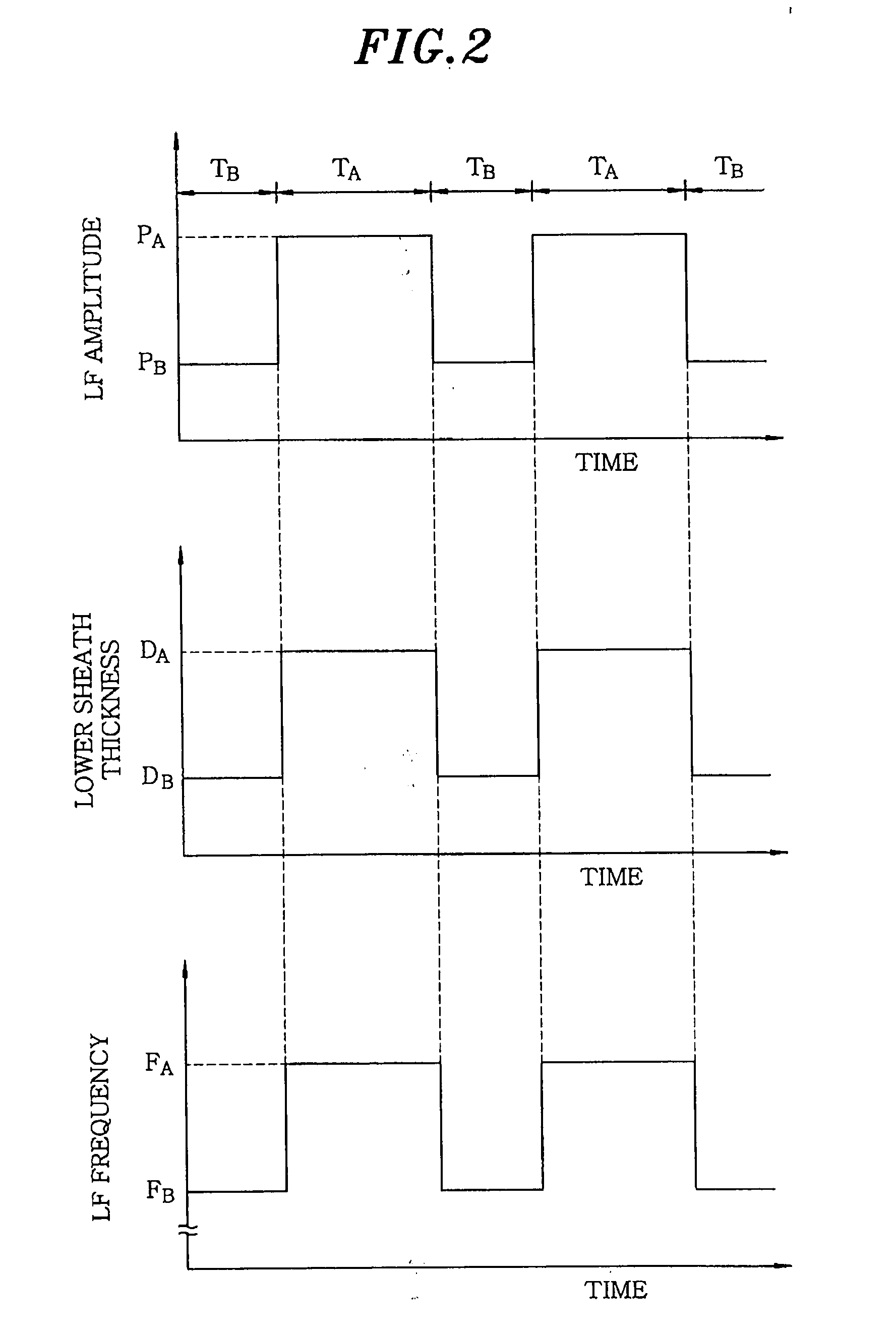
[0138]For example, in the above embodiment, the matching unit response period is set within a period during which the radio frequency power amplitude to be pulse modulated maintains the high level set value (amplitude high level period) TA, and the impedance matching is performed during the amplitude high level period TA. However, when the duty is small, i.e., when the rate of the amplitude high level period TA is smaller compared to that of the amplitude low level period TB in one cycle, the matching unit response period can be set within the am...
PUM
| Property | Measurement | Unit |
|---|---|---|
| Power | aaaaa | aaaaa |
| Frequency | aaaaa | aaaaa |
| Wave power | aaaaa | aaaaa |
Abstract
Description
Claims
Application Information