Solid-state imaging device, production method thereof, and electronic device

Inactive Publication Date: 2009-10-15
SONY CORP
View PDF12 Cites 57 Cited by
  • Summary
  • Abstract
  • Description
  • Claims
  • Application Information

AI Technical Summary

Benefits of technology

[0021]In the electronic device according to the embodiment of the present invention, in the solid-state imaging device, the portion buried into the semiconductor substrate of the second isolation region in the pixel section is shallower than the portion buried into the semiconductor substrate of the first isolation region in the peripheral circuit section, so that adverse effects of stresses and damages by the second isolation region onto the photoelectric conversion element are suppressed. The surface height of the second isolation region in the pixel section is made to be equal to and as low as that of the first isolation region in the peripheral circuit section, so that in fabricating gate electrodes after forming device separation regions, no electrode material remains on the sidewalls of the device separation regions. Because the surface height of the second isolation region in the pixel section is made equal to that of the first isolation region in the peripheral circuit section, the increase of the processing steps due to the difference in the STI structures of the first and second isolation regions can be suppressed to a minimum.
[0022]With the electronic device according to the embodiment of th

Problems solved by technology

With regard to isolation regions in the solid-state imaging device, the former of the abovementioned structures, which forms the regions with the same STI structure in both the pixel section and the peripheral circuit section, is known to have a problem of increasing white spots.
Namely, since the STI isolation regions in the pixel section are formed deep into the semiconductor substrate similarly to the STI isolation regions in the peripheral circuit section, the effects of stresses and damages exerted onto the photodiode increase, and this results in the increase of white spots.
However, in this case, there is a problem of increasing the number of processes, since the formation of the abovementioned diffusion region has to

Method used


Image

  • Solid-state imaging device, production method thereof, and electronic device
  • Solid-state imaging device, production method thereof, and electronic device
  • Solid-state imaging device, production method thereof, and electronic device

Examples


first embodiment

of the Production Method

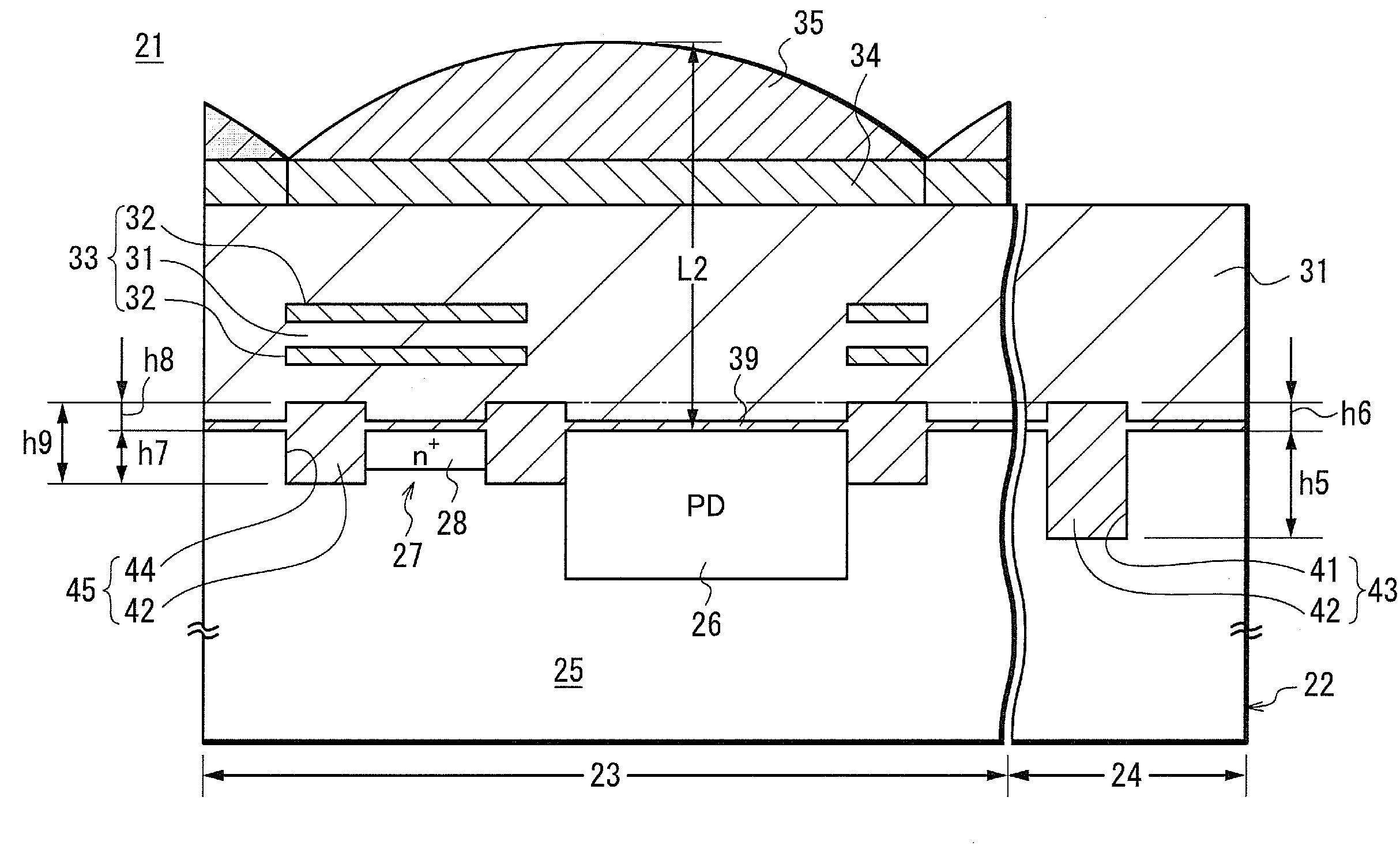
[0116]In the next place, a first embodiment of the production method for the solid-state imaging device according to the present invention will be described with reference to FIGS. 13A through 17J. The present embodiment is adapted to producing the solid-state imaging device according to the aforementioned second embodiment of the solid-state imaging device shown in FIG. 6, in particular to forming isolation regions thereof.

[0117]First, referring to FIG. 13A, a thin insulator film 39 is formed having a first predetermined film thickness on a major surface of a semiconductor substrate 22, and subsequently formed on the insulator film 39 is another insulator film 61 having a second predetermined film thickness with an etching rate different from that of the insulator film 39. As the insulator film 39, a silicon oxide film may be used, for example. As the insulator film 61, a silicon nitride film formed by low pressure CVD of about 100 nm in film thickness may b...

second embodiment

of the Production Method

[0131]In the next place, a second embodiment of the production method for the solid-state imaging device according to the present invention will be described with reference to FIGS. 18A through 22. The present embodiment is adapted to producing the solid-state imaging device according to the aforementioned second embodiment of the solid-state imaging device shown in FIG. 6, in particular to the isolation region thereof.

[0132]First, referring to FIG. 18A, a thin insulator film 39 is formed having a first predetermined film thickness on a major surface of a semiconductor substrate 22, and subsequently formed on the insulator film 39 is another insulator film 61 having a second predetermined film thickness with an etching rate different from that of the insulator film 39. As the insulator film 39, a silicon oxide film may be used, for example. As the insulator film 61, a silicon nitride film formed by the low pressure CVD of about 100 nm in film thickness may be...

third embodiment

of the Production Method

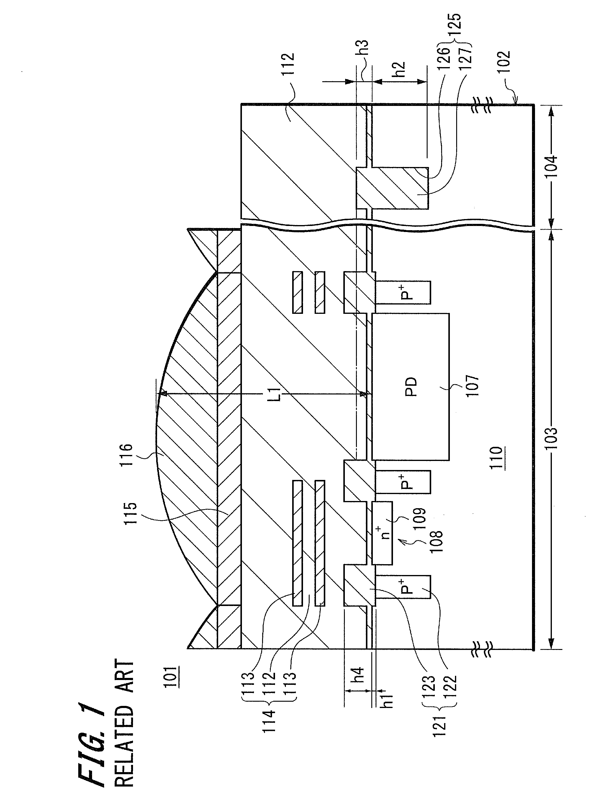
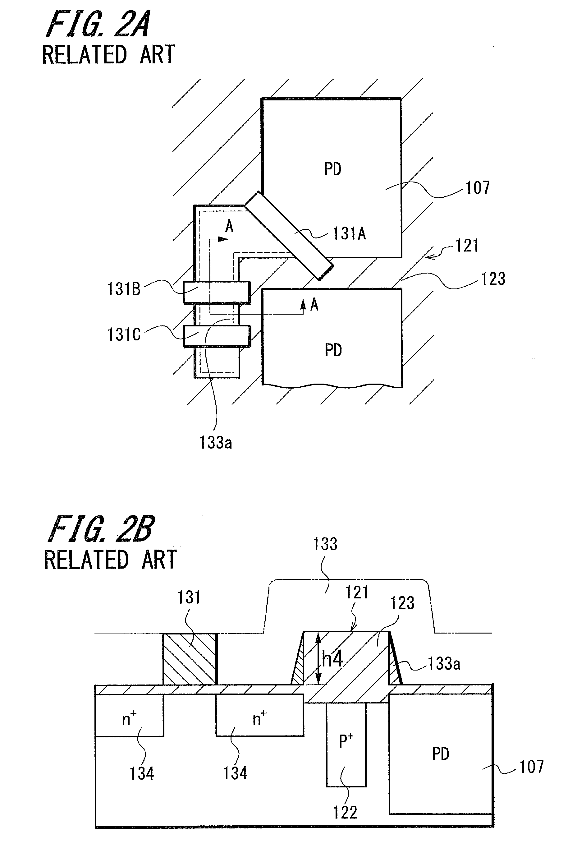
[0142]Next, referring to FIG. 23 through FIG. 25, a third embodiment of the production method for the solid-state imaging device according to the present invention will be described. The present embodiment is adapted to producing the solid-state imaging device 55 according to the fifth embodiment shown in FIG. 9, in particular, to forming the isolation region thereof.

[0143]In the production method according to the third embodiment, first, as illustrated in FIG. 23A, using the processes shown in FIG. 13A through FIG. 15E or in FIG. 18A through FIG. 19D, shallow trenches 44 and deep trenches 41 are formed in pixel sections 23 and peripheral circuit sections 24, respectively. FIG. 23A shows a state that a thin insulator film 39 for example of a silicon oxide film is formed on the surface of a semiconductor substrate 22 where the trenches 44 and 41 are not formed and an insulator film 61 for example of a silicon nitride film is formed thereupon.

[0144]Next, as ill...


PUM


Abstract

Disclosed is a solid-state imaging device which includes a pixel section, a peripheral circuit section, a first isolation region formed with a STI structure on a semiconductor substrate in the peripheral circuit section, and a second isolation region formed with the STI structure on the semiconductor substrate in the pixel section. The portion of the second isolation region buried into the semiconductor substrate is shallower than the portion buried into the semiconductor substrate of the first isolation region, and the height of the upper face of the second isolation region is equal to that of the first isolation region. A method of producing the solid-state imaging device and an electronic device provided with the solid-state imaging devices are also disclosed.

Description

BACKGROUND OF THE INVENTION[0001]1. Field of the Invention[0002]The invention generally relates to solid-state imaging devices, production methods thereof, and electronic devices provided with the solid-state imaging devices.[0003]2. Description of the Related Art[0004]Solid-state imaging devices are broadly classified into amplification type solid-state imaging devices, which are typically illustrated by CMOS (complementary metal-oxide semiconductor) image sensors, and charge transfer type imaging devices, which are typified by CCD (charge-coupled device) image sensors. The solid-state imaging devices have been used extensively in digital still cameras, digital camcorders, etc. In addition, as solid-state imaging devices mounted in mobile devices such as cellular phones with camera, PDA (personal digital assistant), etc., CMOS image sensors are used more frequently in recent years owing to relatively low source voltages and low power consumption characteristics among others.[0005]I...

Claims


Application Information

Patent Timeline
IPC IPC(8): H01L31/0232H01L31/00H01L21/762
CPCH01L27/14609H01L27/14625H01L27/14831H01L27/1463H01L27/14689H01L27/14627
Inventor TATANI, KEIJIMATSUMOTO, TAKUJITATESHITA, YASUSHIKOGA, FUMIHIKONAGANO, TAKASHITOYOSHIMA, TAKAHIROYAMAGUCHI, TETSUJINAKAZAWA, KEIICHIMIYASHITA, NAOYUKINAGAHAMA, YOSHIHIKO
Owner SONY CORP
Why Eureka
Try Eureka