
Eureka
For R&D, Eureka makes reading and utilizing patents & technical documents easy.
Eureka AIR
Designed for self-driven R&D workflows. Generate viable solutions, solve complex R&D challenges, empower your innovation with AI.

Eureka Materials
Designed for material experts only. Revolutionize your material R&D, from search, analyze, to developing new materials.

TechResearch
Generate reliable direction feasibility study reports for your R&D in just a few steps.

TechSeek
Discover and master advanced knowledge NOW. Basics, ideas, possibilities, all at once.

TechMind
As an expert in R&D Theories, TechMind can generates customized viable solutions instantly.

TechRisk
Analyze your overall solution with one click, know your potential R&D risks in advance.

TechMonitor
Get weekly tech updates, stay abreast of the latest tech innovations and key insights.
Organic electroluminescence apparatus
- Summary
- Abstract
- Description
- Claims
- Application Information
AI Technical Summary
Benefits of technology
Problems solved by technology
Method used
Image

Examples
first embodiment
Entire Structure
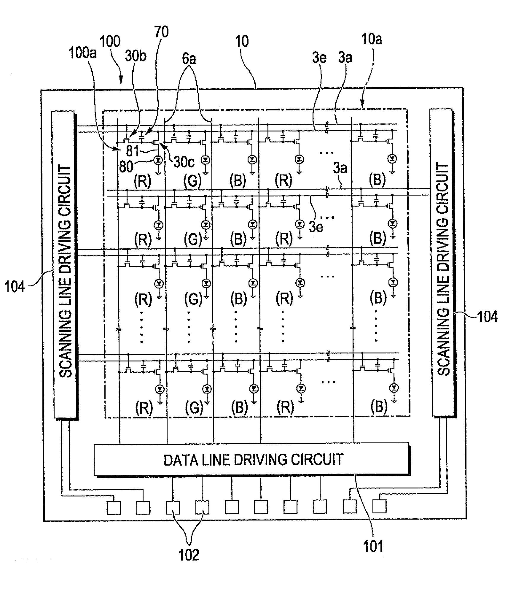
[0034]FIG. 1 is an equivalent circuit diagram illustrating the electric structure of an organic EL apparatus applied with the invention. In the organic EL apparatus 100 shown in FIG. 1, a plurality of scanning lines 3a, a plurality of data lines 6a extending in the direction intersecting the scanning lines 3a, and a plurality of power source lines 3e extending in the direction parallel to the scanning lines 3a are disposed on a first substrate 10. Furthermore, a plurality of pixels 100a is arranged in a matrix in a rectangular pixel region 10a on the first substrate 10. The data lines 6a are connected to a data line driving circuit 101, and the scanning lines 3a are connected to a scanning line driving circuit 104. Each pixel 100a is provided with a switching thin film transistor 30b to supply of scanning signals to a gate electrode via the scanning line 3a, a storage capacitor 70 to store pixel signals supplied from the data line 6a via this switching thin film tran...
second embodiment
[0054]FIG. 5 is a plan view illustrating a positional relationship between the auxiliary wiring layer and the pixels in an organic EL apparatus according to a second embodiment of the invention. Since the basic structure of this embodiment is the same as that of the first embodiment, the same components are designated by the same reference numerals, and the descriptions thereof are omitted. The basic structure of the pixels of the organic EL apparatus of this embodiment will be described with reference to FIGS. 3A and 3B.
[0055]Since the organic EL apparatus of this embodiment is also a top-emission type as in the first embodiment, the second electrode layer 83 shown in FIGS. 3A and 3B is required to be translucent. Accordingly, the second electrode layer 83 has a small thickness, and therefore the electric resistance of the second electrode layer 83 varies depending on the region. Such variation of the electric resistance causes a variation in brightness. Therefore, also in this emb...
third embodiment
[0058]FIG. 6 is a plan view illustrating a positional relationship between the auxiliary wiring layer and the pixels in an organic EL apparatus according to a third embodiment of the invention. Since the basic structure of this embodiment is the same as those of the first and second embodiments, the same components are designated by the same reference numerals, and the descriptions thereof are omitted. The basic structure of the pixels of the organic EL apparatus of this embodiment will be described with reference to FIGS. 3A and 3B.
[0059]Since the organic EL apparatus of this embodiment is also a top-emission type as in the first and second embodiments, the second electrode layer 83 shown in FIGS. 3A and 3B is required to be translucent. Accordingly, the second electrode layer 83 has a small thickness, and therefore the electric resistance of the second electrode layer 83 varies depending on the region. Such variation of the electric resistance causes a variation in brightness. The...
PUM
 Abstract
Description
Claims
Application Information
 - R&D Engineer
- R&D Manager
- IP Professional
- Industry Leading Data Capabilities
- Powerful AI technology
- Patent DNA Extraction
Browse by: Latest US Patents, China's latest patents, Technical Efficacy Thesaurus, Application Domain, Technology Topic, Popular Technical Reports.
© 2024 PatSnap. All rights reserved.Legal|Privacy policy|Modern Slavery Act Transparency Statement|Sitemap|About US| Contact US: help@patsnap.com