
Eureka
For R&D, Eureka makes reading and utilizing patents & technical documents easy.
Eureka AIR
Designed for self-driven R&D workflows. Generate viable solutions, solve complex R&D challenges, empower your innovation with AI.

Eureka Materials
Designed for material experts only. Revolutionize your material R&D, from search, analyze, to developing new materials.

TechResearch
Generate reliable direction feasibility study reports for your R&D in just a few steps.

TechSeek
Discover and master advanced knowledge NOW. Basics, ideas, possibilities, all at once.

TechMind
As an expert in R&D Theories, TechMind can generates customized viable solutions instantly.

TechRisk
Analyze your overall solution with one click, know your potential R&D risks in advance.

TechMonitor
Get weekly tech updates, stay abreast of the latest tech innovations and key insights.
Semiconductor light emitting element and tunable wavelength laser light source
- Summary
- Abstract
- Description
- Claims
- Application Information
AI Technical Summary
Benefits of technology
Problems solved by technology
Method used
Image

Examples
first embodiment
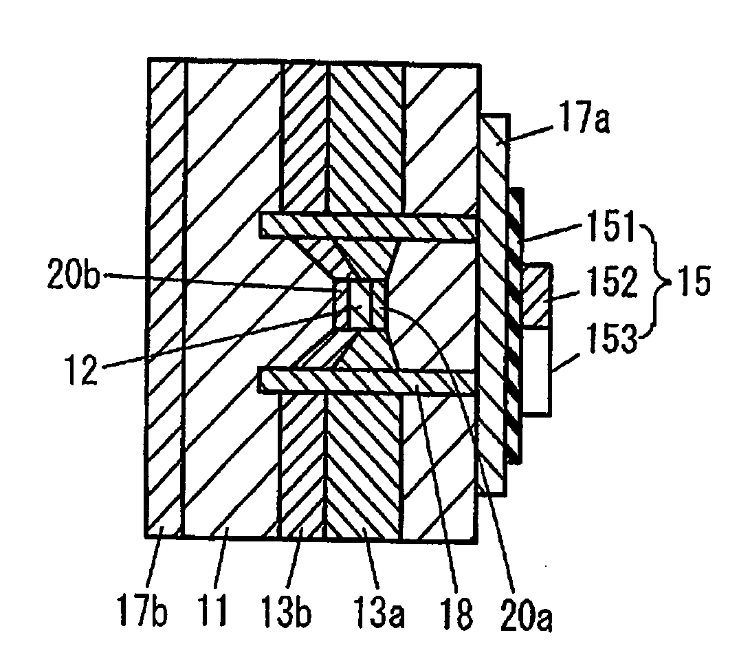
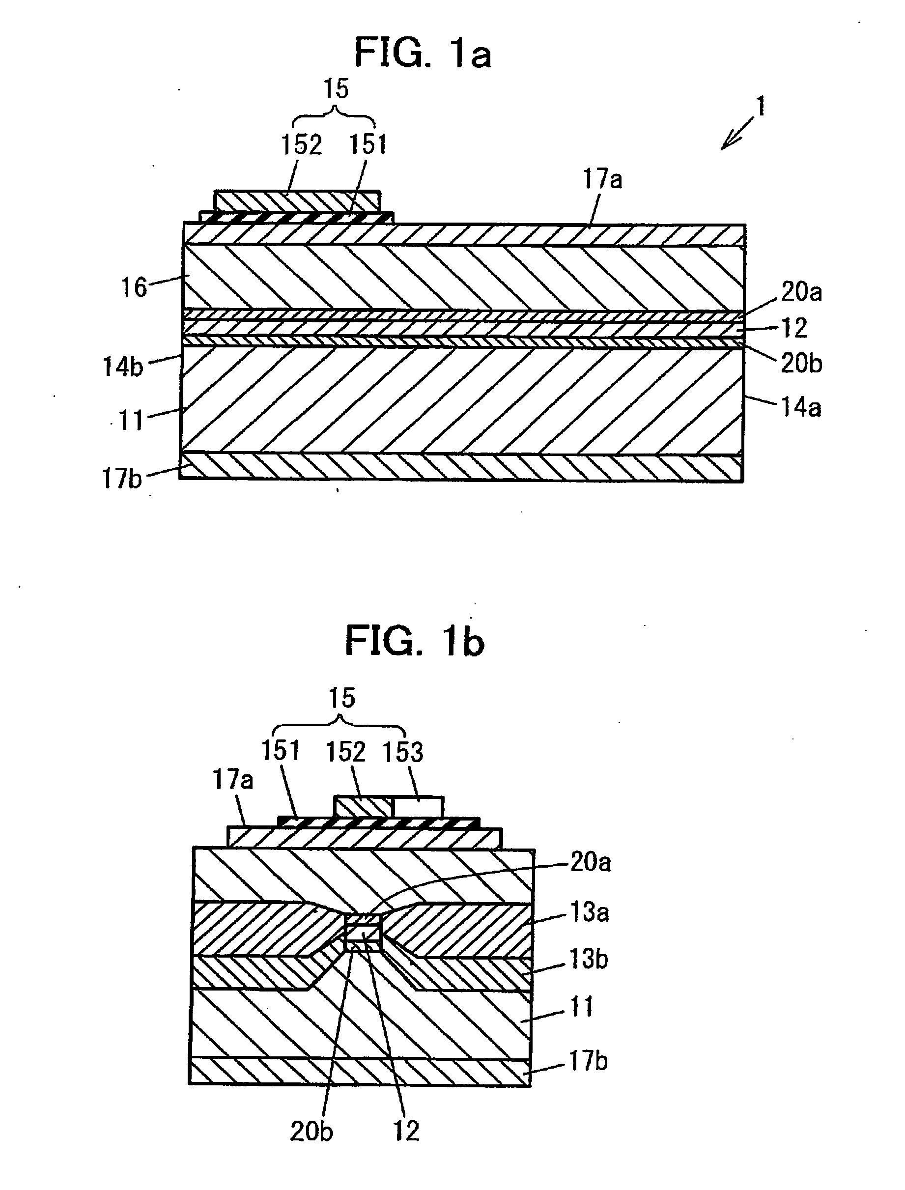
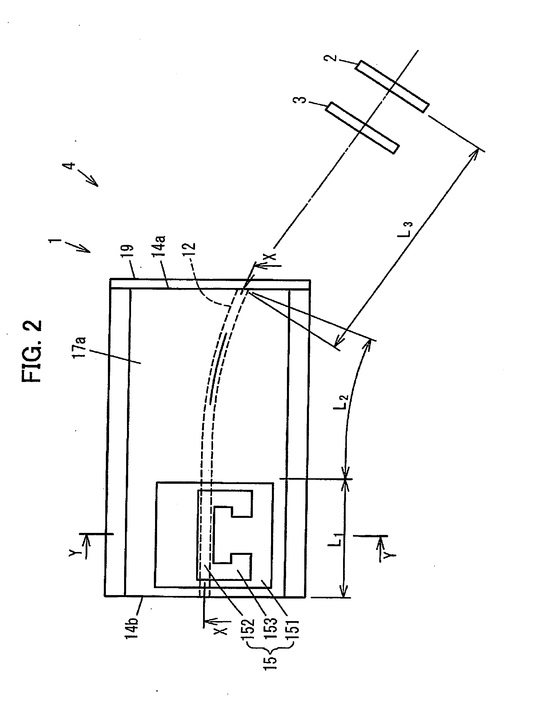
[0056]The first embodiment of a semiconductor light emitting element according to the present invention is shown in FIG. 1. FIG. 1a is a cross-sectional view taken along the line X-X in FIG. 2, FIG. 1b is a cross-sectional view taken along the line Y-Y in FIG. 2.
[0057]The first embodiment of the semiconductor light emitting element 1 comprises a semiconductor substrate 11, an active layer 12 for emitting and propagating light, which is formed in a stripe shape above the semiconductor substrate 11, separate confinement heterostructure (SCH) layers 20a, 20b formed above and below the active layer 12, buried layers 13a, 13b formed on both lateral sides of the SCH layers 20a, 20b and the active layer 12, a cladding layer 16 formed above the SCH layers 20a, 20b and the buried layer 13a, a first electrode 17a formed above the cladding layer 16, and a second electrode 17b formed below the semiconductor substrate 11.
[0058]The two end facets perpendicular to the length direction of the semic...
second embodiment
[0086]The second embodiment of a semiconductor light emitting element according to the present invention is shown in FIG. 4. FIG. 4a is a plan view and FIG. 4b is a cross-sectional view taken along the line Y-Y in FIG. 4a. As shown in those figures, the second embodiment of the semiconductor light emitting element comprises a pair of recessed sections 18 located in crystalline layers at both lateral sides of the predetermined length portion of the active layer, along the direction of light propagation, in addition to the components of the first embodiment.
[0087]The semiconductor light emitting element 1 can improve the heating efficiency of the predetermined length portion of the active layer by utilizing the air in the recessed sections 18 as a heat insulation layer which makes the heat generated at the thin film resistor 152 stored in and around the predetermined length portion of the active layer.
[0088]The distance between the pair of recessed sections 18 needs to be large enough...
third embodiment
[0091]The third embodiment of a semiconductor light emitting element according to the present invention is shown in FIG. 5. FIG. 5a is a plan view, FIG. 5b is a cross-sectional view taken along the line X-X in FIG. 5a, and FIG. 5c is a cross-sectional view taken along the line Y-Y in FIG. 5b.
[0092]The third embodiment of the semiconductor light emitting element having a ridge waveguide comprises a semiconductor substrate 51, an active layer 53 formed above the semiconductor substrate 51 and between SCH layers 52a, 52b which are formed above and below the active layer 53, a cladding layer 54 formed on the SCH layers 52a, a contact layer 55 formed on the cladding layer 54, a first insulating film 56 formed on the contact layer 55, a first electrode 57a formed on the first insulating film 56, and a second electrode 57b formed below the semiconductor substrate 51.
[0093]A ridge section comprising a plurality of layers including the above mentioned cladding layer 54 is formed above the a...
PUM
 Abstract
Description
Claims
Application Information
 - R&D Engineer
- R&D Manager
- IP Professional
- Industry Leading Data Capabilities
- Powerful AI technology
- Patent DNA Extraction
Browse by: Latest US Patents, China's latest patents, Technical Efficacy Thesaurus, Application Domain, Technology Topic, Popular Technical Reports.
© 2024 PatSnap. All rights reserved.Legal|Privacy policy|Modern Slavery Act Transparency Statement|Sitemap|About US| Contact US: help@patsnap.com