Eureka AIR delivers breakthrough ideas for toughest innovation challenges, trusted by R&D personnel around the world.

Perovskite double-band photoelectric detector and preparation method thereof

A technology of perovskite and perovskite precursors, applied in photovoltaic power generation, electric solid-state devices, semiconductor/solid-state device manufacturing, etc., can solve the problems of cumbersome follow-up processing procedures, small film grain size, and poor film quality. Achieve high wavelength selectivity, large grain size, and easy operation

Pending Publication Date: 2021-03-30
PEKING UNIV SHENZHEN GRADUATE SCHOOL
View PDF7 Cites 7 Cited by
  • Summary
  • Abstract
  • Description
  • Claims
  • Application Information

AI Technical Summary

Problems solved by technology

[0014] The purpose of the present invention is to solve the existing problems in the preparation of perovskite thick films in the prior art, such as complicated process, long time consumption, cumbersome follow-up processing procedures, small grain size of the prepared film, rough surface, poor film quality, and general detection performance. lower problems, thereby providing a self-driven perovskite double-band photodetector and its preparation method, the method is easy to operate, low in energy consumption, simple and cheap, conducive to popularization, and the quality of the prepared perovskite film high performance

Method used


Image

  • Perovskite double-band photoelectric detector and preparation method thereof
  • Perovskite double-band photoelectric detector and preparation method thereof
  • Perovskite double-band photoelectric detector and preparation method thereof

Examples


Embodiment 1

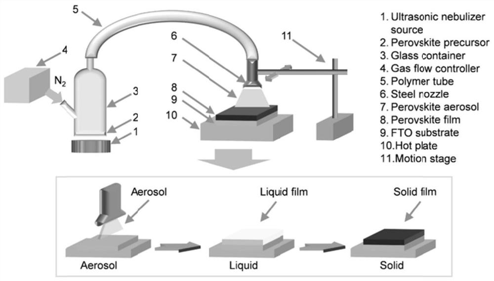
[0054] A kind of perovskite dual-band photodetector, its preparation method comprises the steps:

[0055] (1) Use deionized water, acetone, isopropanol and ethanol to ultrasonically clean the FTO transparent conductive substrate in sequence, and then put it in an oven for 70 o C is dry and ready for use;

[0056] (2) Dissolve 10mmol lead bromide and 10mmol methylamine hydrobromide powder in 12.5ml DMSO and DMF mixed solvent (the volume ratio of DMSO and DMF is 1:1), stir well to obtain MAPbBr 3 The precursor solution (molar concentration is 0.8mol / L); the MAPbBr 3 The precursor solution is atomized to form atomized MAPbBr 3 Precursor solution;

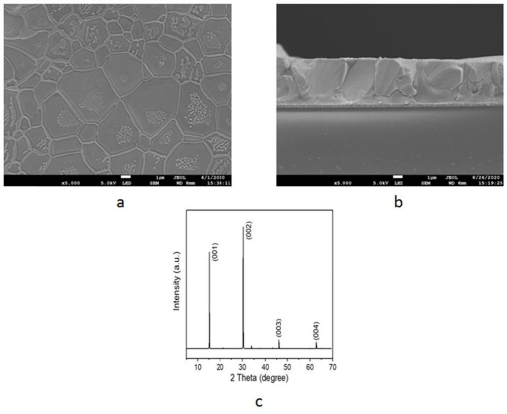
[0057] (3) Place the transparent conductive substrate on the heating table, and the temperature of the heating table rises to 130 o C, the distance between the nozzle and the upper surface of the conductive substrate is adjusted to 3 mm, and the moving speed of the nozzle is controlled to 0.6 cm / s. Use dry nitrogen to pass into th...

Embodiment 2

[0060] A kind of perovskite dual-band photodetector, its preparation method comprises the steps:

[0061] (1) Use deionized water, acetone, isopropanol and ethanol to ultrasonically clean the FTO transparent conductive substrate, and then put it in an oven for 80 o C is dry and ready for use;

[0062] (2) Dissolve 5mmol lead bromide, 5mmol lead chloride, 5mmol methylamine hydrobromide and 5mmol methylamine hydrochloride powder in 12.5ml DMSO and DMF mixed solvent (the volume ratio of DMSO and DMF is 1:1 ), and stir evenly to obtain MAPbBr 1.5 Cl 1.5 The precursor solution (molar concentration is 0.8mol / L); the MAPbBr 1.5 Cl 1.5 The precursor solution is atomized to form atomized MAPbBr 1.5 Cl 1.5 Precursor solution;

[0063] (3) Place the transparent conductive substrate on the heating table, and the temperature of the heating table rises to 140 o C, the distance between the nozzle and the upper surface of the conductive substrate is adjusted to 5 mm, and the moving sp...

Embodiment 3

[0066] A kind of perovskite dual-band photodetector, its preparation method comprises the steps:

[0067] (1) Use deionized water, acetone, isopropanol and ethanol to ultrasonically clean the FTO transparent conductive substrate, and then put it in an oven for 90 o C is dry and ready for use;

[0068] (2) Dissolve 10mmol lead bromide, 9mmol methylamine hydrobromide and 1mmol methylamine hydrobromide powder in 12.5ml DMSO and DMF mixed solvent (the volume ratio of DMSO and DMF is 1:1), and stir evenly to obtain FA 0.1 MA 0.9 PbBr 3 The precursor solution (molar concentration is 0.8mol / L); the FA 0.1 MA 0.9 PbBr 3 The precursor solution is atomized to form atomized FA 0.1 MA 0.9 PbBr 3 Precursor solution;

[0069] (3) Place the transparent conductive substrate on the heating table, and the temperature of the heating table rises to 150 o C, the distance between the nozzle and the upper surface of the conductive substrate is adjusted to 7mm, and the moving speed of the ...


PUM

PropertyMeasurementUnit
particle sizeaaaaaaaaaa
thicknessaaaaaaaaaa
particle sizeaaaaaaaaaa

Abstract

The invention relates to a perovskite thin film, a perovskite double-band photoelectric detector and a preparation method of the perovskite double-band photoelectric detector. The perovskite thin filmprepared according to the invention is uniform in surface and large in grain size, and is much stronger than a perovskite thin film prepared by a freeze drying method or a blade coating method. In addition, the perovskite thin film prepared by the method is controllable in thickness, has higher performance and stability, and meets the condition of double-band detection; meanwhile, the method is convenient to operate, is low in energy consumption, is simple and cheap and is beneficial to popularization. In addition, a dual-band photoelectric detector has a negative broadband detection mode anda positive narrowband detection mode in a short wavelength range and a sub-band gap wavelength range respectively, so that the dual-band photoelectric detector has very high wavelength selectivity. By regulating and controlling the band gap of perovskite, the wavelength range of negative broadband detection and the specific wavelength of positive narrowband detection of the detector can be adjusted. The detector does not need to change the working mode, and has very high application value and potential in the fields of mineral exploration, biological detection, artificial eyeballs, hyperspectral imaging and the like.

Description

technical field [0001] The invention belongs to the technical field of photoelectric materials and relates to photoelectric conversion technology, in particular to a method for preparing a perovskite double-band photodetector. Background technique [0002] A photodetector, also known as a photosensor, is a device that converts light signals into electrical signals. According to the size of the spectral response width, photodetectors can be divided into broadband photodetectors and narrowband photodetectors. Broadband photodetectors are capable of detecting a relatively wide range of wavelengths; in contrast, narrowband photodetectors are photodetectors with high responsivity within a specific and relatively narrow wavelength range, outside which their The response is negligible, so the narrowband photodetector has high wavelength selectivity. Due to the different response width of the two wavelengths, their application ranges are also different. Broadband detectors are ma...

Claims


Application Information

Patent Timeline
Patent Type & Authority Applications(China)
IPC IPC(8): H01L51/48H01L51/42
CPCH10K71/12H10K30/10Y02E10/549
Inventor 杨世和王健肖爽
Owner PEKING UNIV SHENZHEN GRADUATE SCHOOL
Why Eureka
Eureka Blog
Learn More