Digital radiography panel with pressure-sensitive adhesive for optical coupling between scintillator screen and detector and method of manufacture

a technology of digital radiography and optical coupling, applied in the field of digital radiography (dr) systems, can solve the problems of reducing the optical degrading image quality, and reducing the efficiency of image formation, so as to improve the efficiency and resolution of dr panels

Active Publication Date: 2009-10-22
CARESTREAM HEALTH INC
View PDF21 Cites 57 Cited by
  • Summary
  • Abstract
  • Description
  • Claims
  • Application Information

AI Technical Summary

Benefits of technology

[0023]An advantage of the present invention is that it provides a method for optical coupling that enhances DR panel efficiency and resolution and is compatible with a range of materials.
[0024]These and other aspects, objects, features and advantages of the present invention will be more clearly understood and appreciated from a review of the following detailed description of the preferred embodiments and appended claims, and by reference to the accompanying drawings.

Problems solved by technology

However, some drawbacks remain.
This reduces the optical efficiency of image formation due to loss of light, signal crosstalk, and related effects, and tends to degrade image quality.
In practice, however, there is often poor optical coupling between scintillator screen 12 and detector 20. FIG. 2B shows an air gap 44 (dotted outline) between layer 18 of scintillator screen 12 and layer 42 of detector 20.
But for light at larger angles, air gap 44 causes a problem.
The net effects include lost efficiency and reduced spatial resolution (generally measured by the modulation transfer function, MTF).
Generally, solutions that have been proposed for doing this have shown only limited success.
Moreover, although some of the proposed solutions may indeed improve optical coupling, they achieve this at the cost of increased complexity and higher expense or inadvertently introduce other problems.
It is difficult to maintain optical contact between a scintillator screen and a photodiode array throughout the whole detector area at this scale.
However, this type of processing can be complex, may risk damage to the photodiode array and can be very expensive.
Flat panel detector 20 is an expensive device and can cost many thousands of dollars, making it impractical to use as a “substrate” for deposition or coating of materials.
Uniformity of deposition also presents an obstacle that makes this type of solution less than desirable.
Although the FOP provides high-resolution imaging, it suffers a considerable light loss (about 37%).
As with methods (iii) and (iv) just given, this method suffers from the inherently low transmittance of the fiber-optic faceplate.
Each of these optical polymers has accompanying problems.
However, as true fluids, they require containment or will otherwise tend to flow out from the optical interface if unsealed.
However, they are too soft to provide dimensional rigidity, and may swell with prolonged exposure or at elevated temperatures.
However, an additional thermal or radiation process for curing is generally required; such processing can be risky for electronic components of detector 20.
Optical glues exhibit similar problems as optical gels.
It is also difficult to apply a uniform thickness of glue between the scintillator screen and the detector array.
However, this requires a number of added steps for proper adhesion, with some complexity and risk of irregular spacer distribution.
Further difficulties occur in attempting to deposit a columnar scintillator such as CsI directly onto the photodiode array or the fiber-optic faceplate, as noted in (ii), (iv), and (v) above.
This structureless layer would tend to provide significant scattering of light before reaching the photodiode array or the fiber-optic faceplate and degrade the spatial resolution (MTF).
However, as discussed in solution (i) above, an air gap would be very likely if optical contact is not maintained across the detector surface.
This problem would be particularly acute with a large DR detector.
As with the approaches listed in (i) to (iv) above, the solution offered by Homme et al. does not alleviate the problems caused by air gaps at the interface.
Moreover, this solution does not indicate whether or not adhesives are used.
Some types of adhesives, such as epoxies and others, contain compounds that are harmful to CsI crystal material.
While this offers significant advantages for diagnostic imaging, such as in dental imaging, for example, the use of flexible substrates also presents considerable challenges.
One of these challenges is in maintaining good optical coupling between the scintillator and detector components.

Method used


Image

  • Digital radiography panel with pressure-sensitive adhesive for optical coupling between scintillator screen and detector and method of manufacture
  • Digital radiography panel with pressure-sensitive adhesive for optical coupling between scintillator screen and detector and method of manufacture
  • Digital radiography panel with pressure-sensitive adhesive for optical coupling between scintillator screen and detector and method of manufacture

Examples


examples

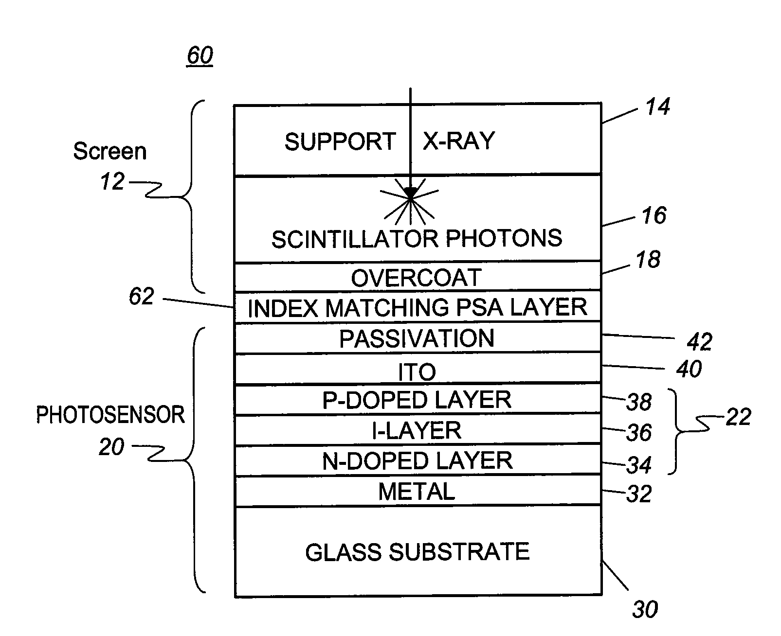
[0064]As described earlier, the optical coupling efficiency depends on the optical properties of each layer for both the scintillator screen and the detector array. Using typical optical parameters for each component in a flat-panel detector, the optical coupling efficiency for various designs are calculated and shown in Tables 1 and 2 for systems using Gd2O2S and CsI screens, respectively.

[0065]These examples show various combinations of phosphor materials, the overcoat layers, the PSA layer, and the passivation layer of the detector array. Results shown in Tables 1 and 2 can be summarized as follows.

[0066](a) If there is an air gap between the scintillator screen and the detector array, the optical coupling efficiency would be reduced by about 60% (Examples 2 and 8 in Table 1, and Examples 12 and 18 in Table 2).

[0067](b) With the use of an index matching PSA layer, the optical coupling efficiency would only decrease by about 2% (Examples 3, 4, 5, and 7 in Table 1, and Examples 13,...


PUM


Abstract

A digital radiography panel has a scintillator screen having a light-exiting surface from a material with a first index of refraction n1 and a photosensor array having a light-accepting surface from a material with a second index of refraction n2. A pressure-sensitive adhesive couples the light-exiting surface of the scintillator screen to the light-accepting surface of the photosensor array and has a third index of refraction that has a value nPSA that either lies in the range between n1 and n2, or substantially matches n1 or n2, or both.

Description

FIELD OF THE INVENTION[0001]This invention generally relates to digital radiography (DR) systems hardware and more particularly relates to indirect DR apparatus having improved optical coupling between scintillator and light detector components.BACKGROUND OF THE INVENTION[0002]Digital radiography is increasingly accepted as an alternative to film-based imaging technologies that rely on photosensitive film layers to capture radiation exposure and thus to produce and store an image of a subject's internal physical features. With digital radiography, the radiation image exposures captured on radiation-sensitive layers are converted, pixel by pixel, to electronic image data which is then stored in memory circuitry for subsequent read-out and display on suitable electronic image display devices.[0003]The perspective view of FIG. 1 shows a partial cutaway view of a small edge portion of an indirect DR panel 10. A scintillator screen 12 responds to incident x-ray radiation by generating vi...

Claims


Application Information

Patent Timeline
Patent Type & Authority Applications(United States)
IPC IPC(8): G01T1/20
CPCG01T1/2018G01T1/20183G01T1/20185
Inventor YIP, KWOK L.
Owner CARESTREAM HEALTH INC
Why Eureka
Try Eureka