Optical device

a technology of optical devices and depletion layers, applied in the field of optical devices, can solve the problems of difficult to satisfy high-speed performance and low-voltage operation, and achieve the effects of small change of depletion layer, low-voltage operation, and increased refractive index

Inactive Publication Date: 2009-10-22
HITACHI LTD
View PDF8 Cites 63 Cited by
  • Summary
  • Abstract
  • Description
  • Claims
  • Application Information

AI Technical Summary

Benefits of technology

[0019]It can be seen from FIG. 8 that as a carrier concentration becomes higher, the change amount of the refractive index increases. As shown in FIG. 6, if the carrier concentration is high, the change of the depletion layer is small. Compared to this, the effect is stronger when an increase in the refractive index changes due to an increase in the change amount of the carrier concentration. In FIG. 8, a refractive index change in a case of a single junction interface is compared with a refractive index change in a case of double junction interfaces. The following can be ...

Problems solved by technology

As described above, in the related art, it is difficult to satisfy high-speed performance, a low-voltage operation (high ...

Method used


Image

  • Optical device
  • Optical device
  • Optical device

Examples


first embodiment

First Vertical Junction Type

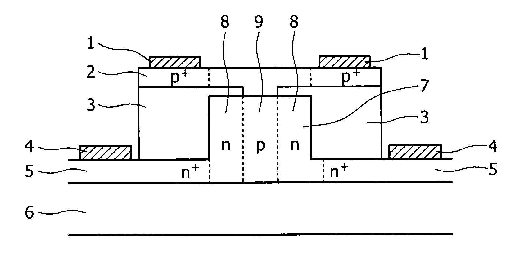
[0038]FIG. 1 shows a cross-sectional view of a waveguide constituting an optical device according to a first embodiment of the present invention. A silicon waveguide 7 has a width of 400 nm and a thickness of 200 nm, and serves as a single mode waveguide with respect to light in a communication wavelength range. An n-p-n junction is formed in the waveguide. All of the doping concentrations of an n-type layer 8 and a p-type layer 9 of the waveguide are controlled to 5×10¹⁷. The waveguide is formed of silicon or is formed by using silicon as a main constituent. Since an n-type part and a p-type part are parts having been doped with impurities, the waveguide can be considered as an example using silicon as a main constituent. The n-type layer 8 of the waveguide is electrically connected to N electrodes through n+-type layers 5 on the left and right sides of the waveguide, respectively. The whole waveguide is covered with a SiO2 layer 3, and a p-type polysili...

second embodiment

Second Vertical Junction Type

[0041]FIGS. 9A and 9B show cross-section views of a waveguide constituting an optical device according to a second embodiment of the present invention. FIGS. 9A and 9B are an overhead view and a top view of the waveguide according to the second embodiment, respectively. As shown in FIGS. 9A and 9B, in the second embodiment, p-n junction interfaces 10 are formed in parallel with a section of the waveguide. A p-type layer 11 of the waveguide is electrically connected to a P electrode through a p+-type layer 16 on a side of the waveguide. On the other hand, the p-type layer 11 and an n+-type layer 13 are completely electrically isolated from each other by an insulating layer 14. Similarly, an n-type layer of the waveguide is electrically connected to an N electrode 12 and is insulated from the p+-type layer 16 on the side of the waveguide.

[0042]Next, an operation of the second embodiment will be described. In the second embodiment, if a reverse bias is appl...

third embodiment

[0043]FIG. 10 shows an example of an MZ interferometer using a waveguide described in the first embodiment, according to a third embodiment of the present invention. Light introduced from a light entrance 23 is divided into two light components at a bifurcation and is guided to phase modulation units 24. Each phase modulation unit 24 is formed with the refractive index modulation structure described in the first embodiment. A voltage applied between a P electrode 22 and an N electrode 23 is changed to change the optical path lengths of upper and lower arms. A phase difference between the upper and lower arms is caused in response to an applied voltage, resulting in a change in the intensity of the light from an exit 23. The MZ interferometer according to the third embodiment is applicable to, for example, a light intensity modulator.


PUM


Abstract

Plural p-n junctions are formed in a waveguide such that they have junction interfaces in a normal direction to a surface of a substrate (to an extending direction of the substrate). Accordingly, a doping concentration changes in only a horizontal direction in the substrate, and it is possible to fabricate using the same processes as those for silicon electronic devices and to perform device fabricating at a low cost. Moreover, two or more junction interfaces are formed in the waveguide and thus an occupied area of the waveguide in a refractive index modulation region expands. Therefore, the efficiency of the refractive index modulation can be improved and a low-voltage operation is possible.

Description

CLAIM OF PRIORITY[0001]The present application claims priority from Japanese patent application serial no. JP 2008-109734, filed on Apr. 21, 2008, the content of which is hereby incorporated by reference into this application.BACKGROUND OF THE INVENTION[0002]1. Field of the Invention[0003]The present invention relates to an optical device, and in particular, to a configuration of a light control device, such as an optical modulator, an optical switch, and an attenuator, using silicon for a component.[0004]2. Description of the Related Art[0005]A technique that is called silicon photonics has been currently in the spotlight. A concept of an optical device using, as a material, silicon, which can be easily obtained and is inexpensively processed, has been proposed from the past. However, an actual light emitting device or a light control device using silicon has been slowly developed due to the following reasons: silicon has extremely low luminous efficacy, difficulties in growing qua...

Claims


Application Information

Patent Timeline
IPC IPC(8): G02B6/12
CPCG02B6/12004G02B6/12007G02F2203/15G02F2001/0152G02F2202/105G02F1/025G02F1/0152
Inventor HOSOMI, KAZUHIKOSUGAWARA, TOSHIKIMATSUOKA, YASUNOBUARIMOTO, HIDEOSAITO, SHINICHI
Owner HITACHI LTD
Why Eureka
Try Eureka