Protection circuit
a protection circuit and circuit technology, applied in the field of protection circuits, can solve the problems of increased manufacturing cost, difficulty in preventing a reduction in the breakdown voltage of a device, etc., and achieve the effect of suppressing the voltag
- Summary
- Abstract
- Description
- Claims
- Application Information
AI Technical Summary
Benefits of technology
Problems solved by technology
Method used
Image
Examples
first embodiment
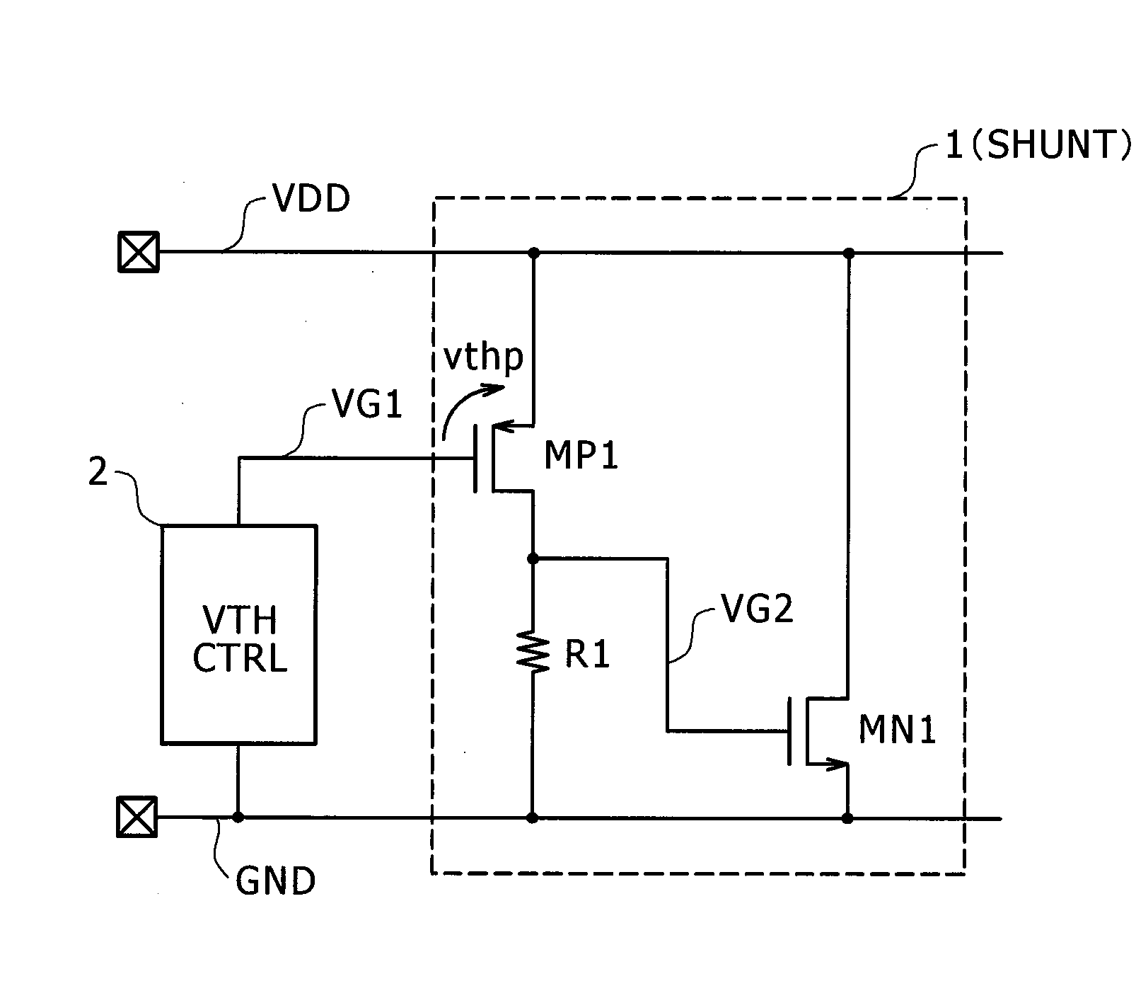
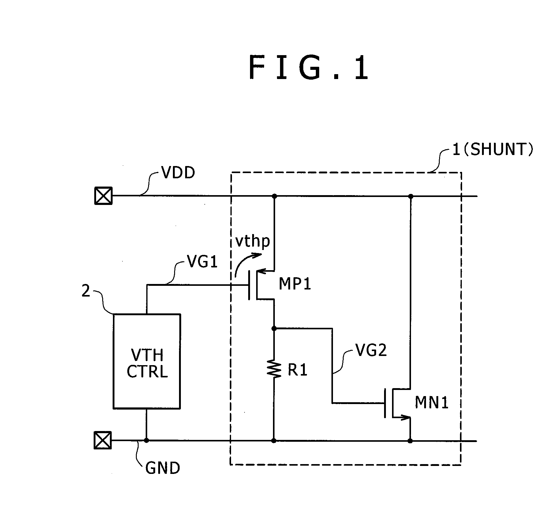
[0033]FIG. 1 is a diagram illustrating a protection circuit according to a first embodiment of the invention. A PMOS transistor MP1 has a source terminal connected to a power supply VDD and a gate terminal receiving a control signal VG1 generated by a control circuit 2 on the basis of a power supply GND, and serves as a sensing circuit for sensing a potential difference between the power supply VDD and the power supply GND. When VDD−GND≧VG1+vthp, in which vthp denotes a threshold voltage of the PMOS transistor MP1, is established, the PMOS transistor MP1 is turned on and thus a current flows to the resistor R1 so as to increase the internal signal VG2 which was at a power GND level. Accordingly, an NMOS transistor MN1 having a drain terminal and a source terminal connected to the power supply VDD and the power supply GND, respectively, and a gate terminal receiving the internal signal VG2 is turned on so as to short-circuit the power supply VDD and the power supply GND. Therefore, w...
second embodiment
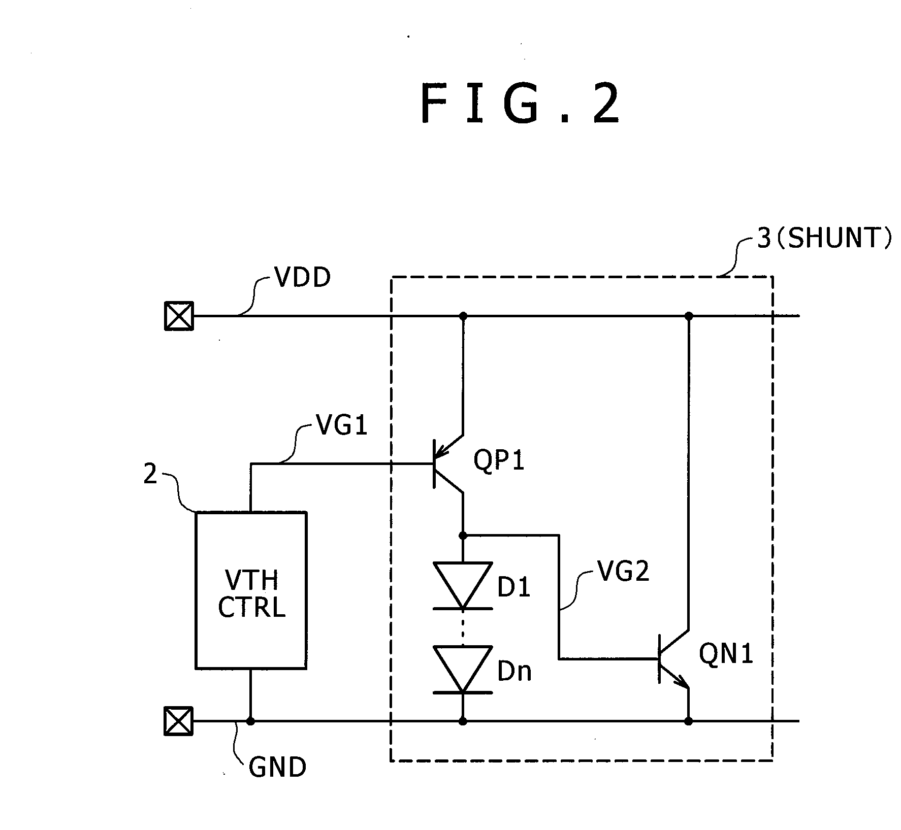
[0034]FIG. 2 is a diagram illustrating a protection circuit according to a second embodiment of the invention. A basic configuration and a basic operation are the same as those of the first embodiment of FIG. 1 and thus a description thereof is omitted. Different functional parts will be described. When a PNP transistor is prepared, the PMOS transistor MP1 of FIG. 1 can be substituted with the PNP transistor. Further, when an NPN transistor is prepared, the NMOS transistor MN1 can be substituted with an NPN transistor. Similarly, the resistor R1 can be substituted with forward diodes Dn cascaded in multiple stages, a resistor connected in series with a forward diode, or a resistor using an ON resistance of a MOS transistor. Such substitution may be applied to any one of the devices according to the characteristics or circuit operations of the devices.
third embodiment
[0035]FIG. 3 is a diagram illustrating a protection circuit according to a third embodiment of the invention. A basic configuration and a basic operation are the same as those of the first embodiment of FIG. 1 and thus a description thereof is omitted. Different functional parts will be described. In FIG. 1, the drain terminal of the NMOS transistor MN1 is connected to the power supply VDD. However, in the third embodiment, forward diodes Dn cascaded in multiple stages are provided between the power supply VDD and the drain terminal. The stage number of the diodes Dn is adjusted such that the sum of forward voltages thereof becomes a value approximate to the potential difference between the power supply VDD and the power supply GND during a normal operation. Therefore, even when turning off of the NMOS transistor MN1 is delayed, the voltage between the power supplies is clamped around a normal operation voltage by the diodes Dn, whereby the voltage between the power supplies is prev...
PUM
 Abstract
Description
Claims
Application Information


