Process kit for RF physical vapor deposition

a technology of physical vapor deposition and process kit, which is applied in vacuum evaporation coating, electrolysis components, coatings, etc., can solve the problems of inability to provide the necessary electrical isolation, lack of multiple grounding points, and potential source of particulate contamination in conventional designs

Active Publication Date: 2009-11-05
APPLIED MATERIALS INC
View PDF31 Cites 31 Cited by
  • Summary
  • Abstract
  • Description
  • Claims
  • Application Information

AI Technical Summary

Problems solved by technology

As the rings and shield periodically contact each other as the substrate support pedestal raises and lowers between transfer and process positions, conventional designs are potential source of particulate contamination.
Further, existing shield designs often lack multiple grounding points and are often unable to provide the necessary electrical isolation to prevent arcing from RF source plasma.

Method used


Image

  • Process kit for RF physical vapor deposition
  • Process kit for RF physical vapor deposition
  • Process kit for RF physical vapor deposition

Examples


Embodiment Construction

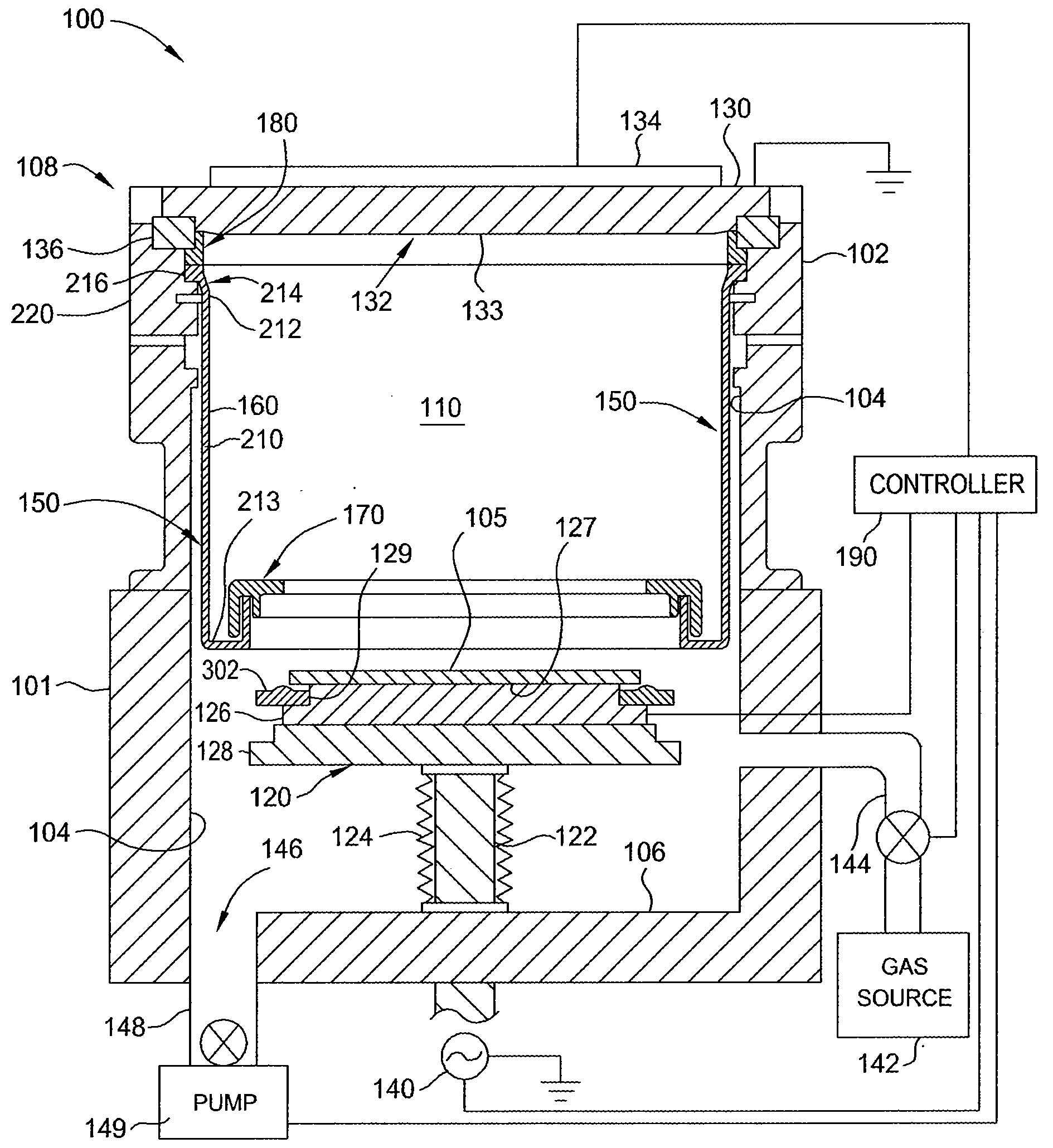
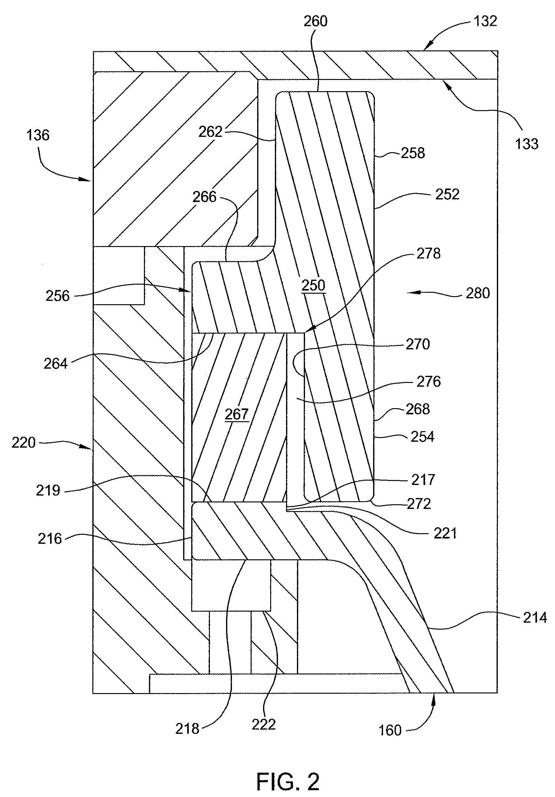
[0029]Embodiments of the invention generally provide a process kit for use in a physical deposition chamber (PVD) chamber. In one embodiment, the process kit provides a reduced RF return path contributing to a reduction in RF harmonics and stray plasma outside the process cavity, which promotes greater process uniformity and repeatability along with longer chamber component service life. In one embodiment, the process kit provides an isolator ring designed to reduce electrical shorts between the chamber walls and the target.

[0030]FIG. 1 depicts an exemplary semiconductor processing chamber 100 having one embodiment of a process kit 150 capable of processing a substrate 105. The process kit 150 includes a one-piece ground shield 160, an interleaving cover ring 170, and an isolator ring 180. In the version shown, the processing chamber 100 comprises a sputtering chamber, also called a physical vapor deposition or PVD chamber, capable of depositing titanium or aluminum oxide on a subst...


PUM

PropertyMeasurementUnit
inner diameteraaaaaaaaaa

Abstract

Embodiments of the invention generally relate to a process kit for a semiconductor processing chamber, and a semiconductor processing chamber having a kit. More specifically, embodiments described herein relate to a process kit including a cover ring, a shield, and an isolator for use in a physical deposition chamber. The components of the process kit work alone and in combination to significantly reduce particle generation and stray plasmas. In comparison with existing multiple part shields, which provide an extended RF return path contributing to RF harmonics causing stray plasma outside the process cavity, the components of the process kit reduce the RF return path thus providing improved plasma containment in the interior processing region.

Description

CROSS-REFERENCE TO RELATED APPLICATIONS[0001]This application claims benefit of U.S. Provisional Patent Application Ser. No. 61 / 050,112, filed May 2, 2008, which is hereby incorporated by reference in its entirety.BACKGROUND OF THE INVENTION[0002]1. Field of the Invention[0003]Embodiments of the invention generally relate to a process kit for a semiconductor processing chamber, and a semiconductor processing chamber having a kit. More specifically, embodiments of the invention relate to a process kit including a cover ring, a shield, and isolator for use in a physical deposition chamber.[0004]2. Description of the Related Art[0005]Physical vapor deposition (PVD), or sputtering, is one of the most commonly used processes in the fabrication of electronic devices. PVD is a plasma process performed in a vacuum chamber where a negatively biased target is exposed to a plasma of an inert gas having relatively heavy atoms (e.g., argon (Ar)) or a gas mixture comprising such inert gas. Bombar...

Claims


Application Information

Patent Timeline
Patent Type & Authority Applications(United States)
IPC IPC(8): C23C14/34
CPCC23C14/35H01J37/32642H01J37/32623H01J37/32082H01J37/32651H01J37/3441
Inventor YOUNG, DONNYHAWRYLCHAK, LARA
Owner APPLIED MATERIALS INC
Why Eureka
Try Eureka