

Poly-Crystalline Layer Structure for Light-Emitting Diodes
- Summary
- Abstract
- Description
- Claims
- Application Information
AI Technical Summary
Benefits of technology
Problems solved by technology
Method used
Image

Examples
Embodiment Construction
[0017]The making and using of the presently preferred embodiments are discussed in detail below. It should be appreciated, however, that the present invention provides many applicable inventive concepts that can be embodied in a wide variety of specific contexts. The specific embodiments discussed are merely illustrative of specific ways to make and use the invention, and do not limit the scope of the invention.
[0018]The present invention will be described with respect to preferred embodiments in a specific context, namely a light-emitting diode. The invention may also be applied, however, to other epitaxially grown layers.
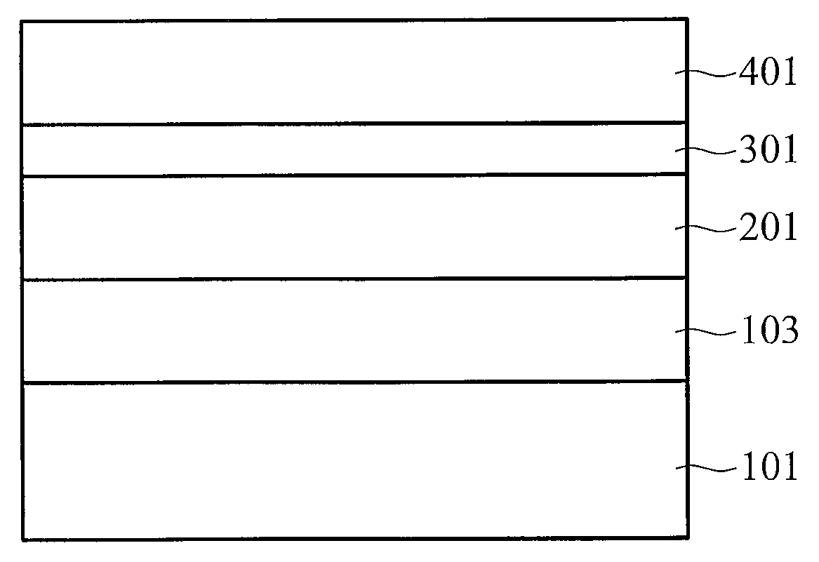
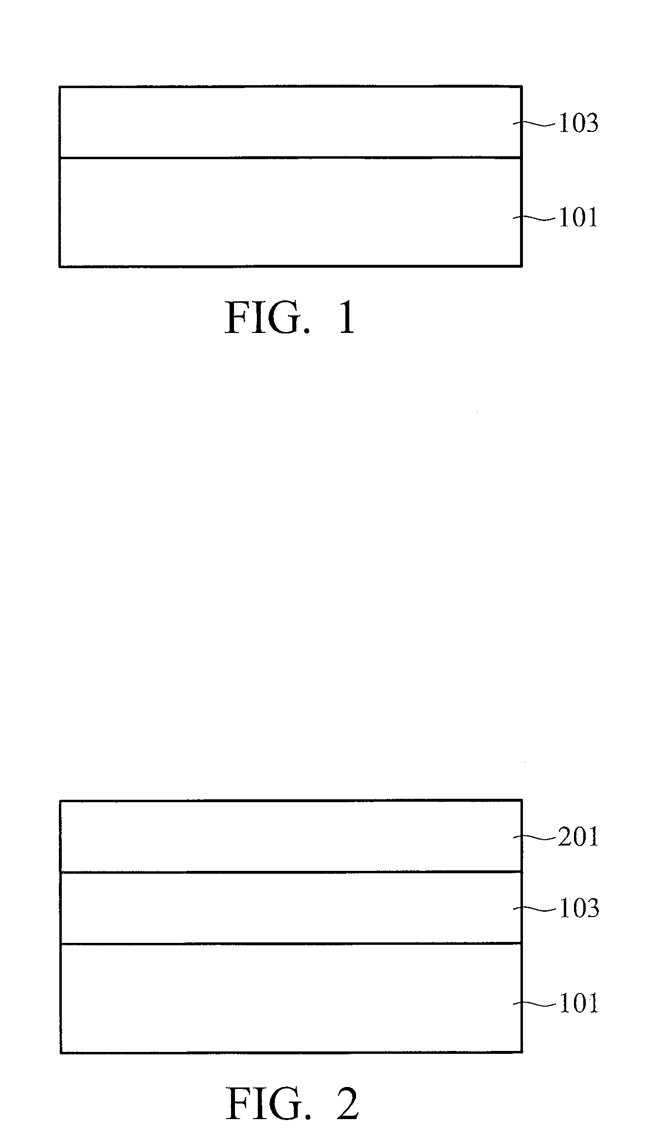
[0019]With reference now to FIG. 1, there is shown a substrate 101 with a poly-crystalline layer 103 over the substrate 101. Substrate 101 preferably comprises a non-conductive substrate such as undoped silicon, sapphire, MgAl2O4, oxide monocrystalline, combinations of these, or the like. Alternatively, a conductive substrate doped to a desired conductivity, such ...
PUM
 Abstract
Description
Claims
Application Information