Current negative-feedback circuit and dc-dc converter using the circuit

a negative-feedback circuit and current-feedback technology, applied in the direction of dc-dc conversion, power conversion systems, instruments, etc., can solve the problems of difficult to solve oscillation problems, affecting control operations, and the inability to use mask signal methods for recent dc-dc converters, etc., to achieve the effect of reducing the manufacturing cost of an ic, speeding up the current negative-feedback circuit, and reducing the influence of on/off noise o

Inactive Publication Date: 2009-11-05
FUJI ELECTRIC CO LTD
View PDF4 Cites 40 Cited by
  • Summary
  • Abstract
  • Description
  • Claims
  • Application Information

AI Technical Summary

Benefits of technology

[0022]According to an aspect of the present invention, a current negative-feedback circuit of the present invention detects current proportional to the current during the charge period of the inductance by a current mirror circuit and generates a sawtooth-shaped waveform, adding the output current of the current mirror circuit to the charge current of a sawtooth-shaped waveform generation circuit. Therefore, the speed of the current negative-feedback circuit can be improved by a simple circuit, the influence of the on / off noise of the switching device can be reduced without providing any special additional circuits, and the manufacturing cost of an IC can be reduced.
[0023]According to an aspect of the present invention, a DC-DC converter uses the above-described current negative-feedback circuit of the present invention. The DC-DC converter contains a current mirror circuit which detects current almost proportional to the inductance current during the charging period of an inductance or a current that is a quadratic function of the inductance current during the charging period of an inductance and outputs the current to a sawtooth-shaped waveform generation circuit, and the DC-DC converter generates a sawtooth-shaped waveform by adding the output current of the current mirror circuit to the charge current of the sawtooth-shaped waveform generation circuit. Therefore, the DC-DC converter can generate / output current almost proportional to an inductance current so as to perform current mode control at high speed or can generate / output current that is the quadratic function of the charge current during the charging period of an inductance by a simple circuit. Simultaneously, the DC-DC converter can reduce the influence of the on / off noise of the switching device without providing any special additional circuit and can reduce the manufacturing cost.

Problems solved by technology

Generally, it is difficult to solve the problem of oscillation due to phase rotation by the negative feedback of only a voltage component.
However, if a time of the noise superimposed is long, it affects the control operation.
Therefore, sometimes the mask signal method cannot be used for a recent DC-DC converter whose clock frequency is high, that is, 1 MHz or more.
The second problem of the configuration of the conventional current negative-feedback circuit and the DC-DC converter using the circuit that are illustrated in FIG. 1 is that a Current Detect 11 whose slew rate (SR) is high is required since when the clock frequency increases, the operation frequency of the Current Detect 11 also increases.
Although Patent document 1 discloses a technology for detecting current via the combination of a detection resistor and an operational amplifier that are provided on the high-potential side, this technology corresponds to the conventional art cited in this specification and is not useful for the solution of the above-described problems with the conventional art.
Although Patent document 2 discloses a technology for suppressing the sub-harmonic oscillation of a pulse signal, it fails to disclose how to solve the slew rate SR problem and the switching noise problem.

Method used


Image

  • Current negative-feedback circuit and dc-dc converter using the circuit
  • Current negative-feedback circuit and dc-dc converter using the circuit
  • Current negative-feedback circuit and dc-dc converter using the circuit

Examples


first preferred embodiment

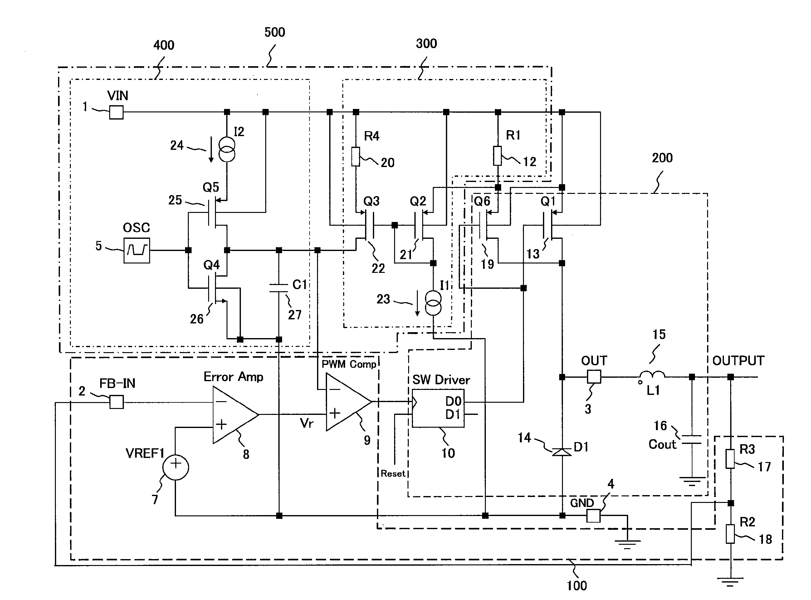
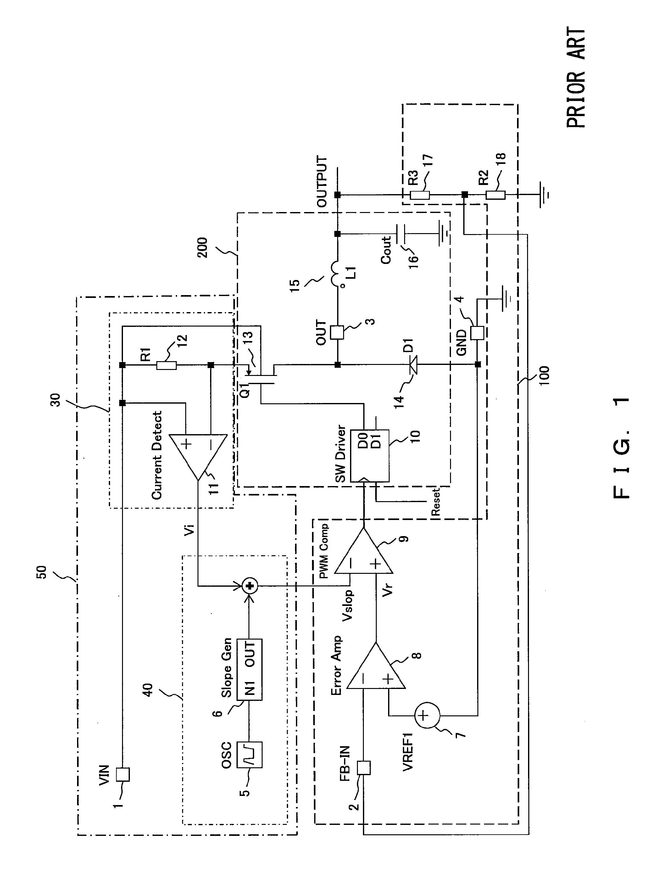
[0034]FIG. 5 shows the first preferred embodiment of a current negative-feedback circuit and a DC-DC converter using the circuit, according to the preferred embodiment of the present invention. In FIG. 5, the same reference numerals are attached to components common to those illustrated in FIG. 1. As in FIG. 1, the Error Amp 8, the reference voltage VREF1 (7), the PWM Comp 9 and the resistors R3 (17) and R2 (18) constitute the FB control unit 100, and the SW driver 10, the switching devices Q1 (13) and Q6 (19), the inductor L1 (15), the diode D1 (14), and the output capacitor Cout 16 constitute the output generation unit 200.

[0035]In FIG. 5, a constant current source I2 (24), a P-ch MOSFET Q5 (25) that is the first switching device and that becomes a charge route to a capacitor C1 (27), an N-ch MOSFET Q4 (26) that is the second switching device and that becomes a discharge route to a capacitor C1 (27), and a capacitor C1 (27) constitute a sawtooth-shaped waveform generation unit 400...

second preferred embodiment

[0055]FIG. 6 shows the second preferred embodiment of a current negative-feedback circuit and a DC-DC converter using the circuit, according to the preferred embodiment of the present invention, in which the switching device Q1 (13) illustrated in FIG. 5 is composed of an N-ch MOSFET instead of the P-ch MOSFET. In FIG. 6, the same reference numerals are attached to components common to those in FIG. 5. The Error Amp 8, the reference voltage VREF1 (7), the PWM Comp 9, and the resistors R3 (17) and R2 (18) constitute the FB control unit 100, and the SW Driver 10, the switching device Q1 (13) composed of an N-ch MOSFET, the inductor L1 (15), the diode D1 (14), and the output capacitor Cout 16 constitute the output generation unit 220, which is almost the same as in FIG. 5. As in FIG. 5, the current detection unit 300 and the sawtooth-shaped waveform generation unit 400 constitute the current negative-feedback circuit 500 according to the preferred embodiment of the present invention.

[0...

third preferred embodiment

[0057]In the second preferred embodiment illustrated in FIG. 6, as described above, it is feared that since the inductance current IL1 is large, the value of the current detection resistor R1 (12) will be so small that it will be difficult to manufacture it as an IC. Therefore, in the third preferred embodiment of a current negative-feedback circuit and a DC-DC converter using the circuit according to the preferred embodiment of the present invention illustrated in FIG. 7, a switching device Q6 (19), which is the same as the switching device Q1 (13) except that it has a gate width of 1 / N that of the switching device Q1 (13), is connected to the switching device Q1 (13) in parallel (their gates and sources are commonly connected), the current detection resistor R1 (12) is inserted between the drain of the switching device Q6, and the input power terminal VIN1 and a current almost proportional to the charge current of the inductance is generated / outputted via the current mirror circui...


PUM


Abstract

A current negative-feedback circuit comprises a current detection unit and a sawtooth-shaped waveform generation unit. The current detection unit comprises a first P-ch MOSFET Q2 and a second P-ch MOSFET Q3 which constitute a current mirror circuit, a current adjustment resistor R4, a current detection resistor R1, and a constant current source I1. The current mirror circuit outputs current almost proportional to the charge current of an inductance via a switching device or outputs a current which is the quadratic function of the charge current of an inductance. The sawtooth-shaped waveform generation means adds the constant charge current of the constant current source I2 and the current output from the current mirror circuit, charges the capacitor C1, and generates a sawtooth-shaped waveform.

Description

BACKGROUND OF THE INVENTION[0001]1. Field of the Invention[0002]The embodiments discussed herein are related to a current negative-feedback circuit for performing control in a current mode and to a DC-DC converter using the circuit, and more particularly are related to a current negative-feedback circuit capable of detecting current almost proportionally to inductance current for current mode control or capable of being a quadratic function of inductance current at a high speed using a simple circuit and capable of reducing the influence of switching noise and a DC-DC converter using the circuit.[0003]2. Description of the Related Art[0004]FIG. 1 shows configurations of a conventional current negative-feedback circuit and a buck type DC-DC converter using the circuit. There are many types of DC-DC converters, such as a buck type, a boost type, a buck / boost type, and an invert type, but the buck type DC-DC converter shown in FIG. 1 is described as a representative.[0005]In FIG. 1, re...

Claims


Application Information

Patent Timeline
Patent Type & Authority Applications(United States)
IPC IPC(8): G05F1/10
CPCH02M3/156H02M2001/0025H02M2001/0009H02M1/0009H02M1/0025
Inventor NAKAHASHI, YASUNORIYAMANE, SATOSHI
Owner FUJI ELECTRIC CO LTD
Why Eureka
Try Eureka