

Sensing circuit, display device and electronic apparatus
a technology of sensing circuit and display device, which is applied in the direction of instruments, transmission systems, computing, etc., can solve the problems of difficult to set the capacitance to a target value, the sensitivity of sensing is varies, and the ordinary sensing circuit is not easy to achieve. , to achieve the effect of reducing the variation of the sensitivity of the sensing circui
- Summary
- Abstract
- Description
- Claims
- Application Information
AI Technical Summary
Benefits of technology
Problems solved by technology
Method used
Image

Examples
first embodiment
A. First Embodiment
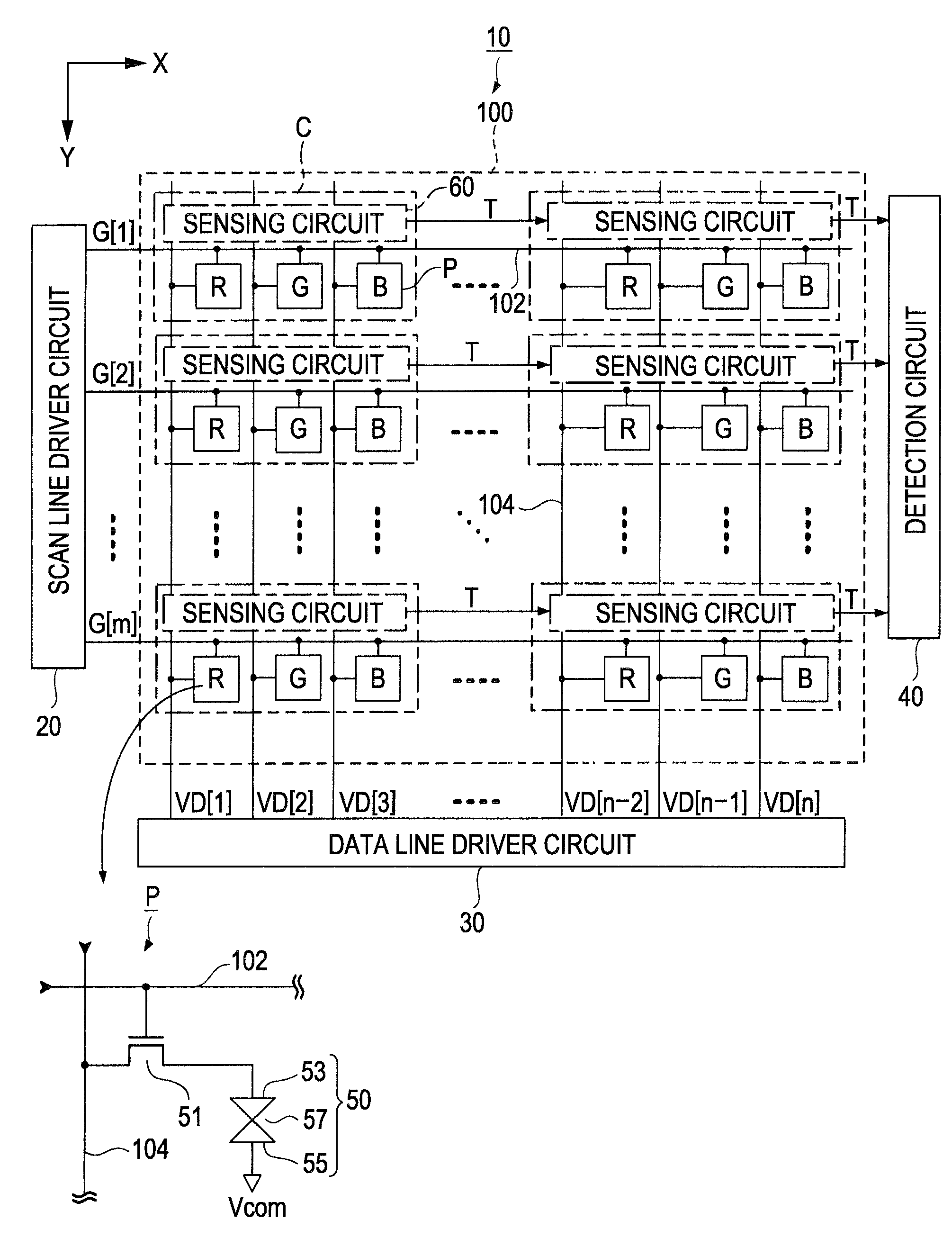
[0035]FIG. 1 is a block diagram of a display device 10 of a first embodiment of the invention. The display device 10 has a pixel area 100, a scan line driver circuit 20, a data line driver circuit 30 and a detection circuit 40. The pixel area 100 is formed by a plurality of pixels arranged on a plane. The scan line driver circuit 20 and the data line driver circuit 30 are configured to drive each of pixel circuits P. The detection circuit 40 is configured to detect contact between an object and the display device 10. As shown in FIG. 1, m scan lines 102 extending in an X-direction and n data lines 104 extending in a Y-direction, which is perpendicular to the X-direction, are arranged in the pixel area 100 (m and n are natural numbers no less than two). Each of the pixel circuits P is arranged at a position corresponding to an intersection of one of the scan lines 102 and one of the data lines 104. Thus, the pixel circuits P are arranged to form an m (vertical) tim...
second embodiment
B. Second Embodiment
[0061]FIG. 10 is a plan view specifically showing a configuration of the display device 10 of a second embodiment (corresponding to FIG. 7 of the first embodiment). As shown in FIG. 10, the first electrode 64 and the second electrode 65 of the sensing circuit 60 of the second embodiment are formed from different layers and arranged to face each other. FIG. 11 is a cross-sectional view of the sensing circuit 60 as viewed from a line “XI-XI” shown in FIG. 10 (corresponding to FIG. 8 of the first embodiment). As shown in FIG. 11, the second electrode 65 is arranged on the face of the third insulation layer Fa3. The second electrode 65 is electrically connected to the conductive layer 116 through the contact hole CH3 as similarly to the first embodiment. As shown in FIG. 11, the second electrode 65 is covered by a fourth insulation layer Fa4. The first electrode 64 is arranged to face the second electrode 65 on a face of the fourth insulation layer Fa4. Although not ...
third embodiment
C. Third Embodiment
[0065]FIG. 13 is a plan view specifically showing a configuration of the display device 10 of a third embodiment (corresponding to FIG. 7 and FIG. 10). As shown in FIG. 13, the sensing circuit 60 of the third embodiment is configured differently from that of the second embodiment in that the first electrode 64 and the second electrode 65 are formed from different layers and that the first electrode 64 and the second electrode 65 are shaped like the teeth of a comb each and arranged to mesh with each other on the plan view. Each of other portions is a same as the corresponding one of the second embodiment, and its explanation is omitted.
[0066]FIG. 14 is a cross-sectional view of the of the sensing circuit 60 as viewed from a line “XIV-XIV” shown in FIG. 13 (corresponding to FIG. 8 and FIG. 11 of the first embodiment). The first electrode 64 of the third embodiment is shaped in such a way that an area of a portion overlapping the second electrode 65 is smaller than ...
PUM
 Abstract
Description
Claims
Application Information