Method for performing a shelf lifetime acceleration test

a technology of integrated circuits and acceleration tests, which is applied in the direction of individual semiconductor device testing, semiconductor/solid-state device testing/measurement, instruments, etc., can solve the problems of difficult to form a bond unreliable bonding between a bondwire and a bondpad, and contaminated surface of a bondpad, so as to avoid the formation of water droplets on the surface of the wafer, the effect of avoiding the introduction of ar

Inactive Publication Date: 2009-11-12
CHARTERED SEMICONDUCTOR MANUFACTURING +1
View PDF15 Cites 10 Cited by
  • Summary
  • Abstract
  • Description
  • Claims
  • Application Information

AI Technical Summary

Benefits of technology

[0023]Embodiments of the invention have the advantage of avoiding introduction of artefacts. This is because dewing-free conditions are maintained during the course of a test according to embodiments of the invention. By maintaining dewing-free conditions, the formation of water droplets on the surface of the wafer is avoided.

Problems solved by technology

The problem exists that the surface of a bondpad can become contaminated.
If the amount of contamination exceeds a critical value, bonds formed between a bondwire and a bondpad may be unreliable and susceptible to breakage.
In some cases, if the amount of contamination is excessive, it may be difficult to form a bond between a bondwire and a bondpad.
During storage of the wafer, the amount of AlxFyOz, can increase until the formation of reliable bonds to a bondpad is no longer possible.
The requirement to perform a shelf lifetime test on a test wafer of a batch of wafers before shipping the batch to a customer introduces a significant delay in the delivery of the batch.
Furthermore, the results of the traditional test are found to be unrepeatable in a reliable manner.
This introduces a level of uncertainty in the determination whether a given batch of wafers may be warrantied as suitable for being stored for a give period of time.

Method used


Image

  • Method for performing a shelf lifetime acceleration test
  • Method for performing a shelf lifetime acceleration test
  • Method for performing a shelf lifetime acceleration test

Examples


first embodiment

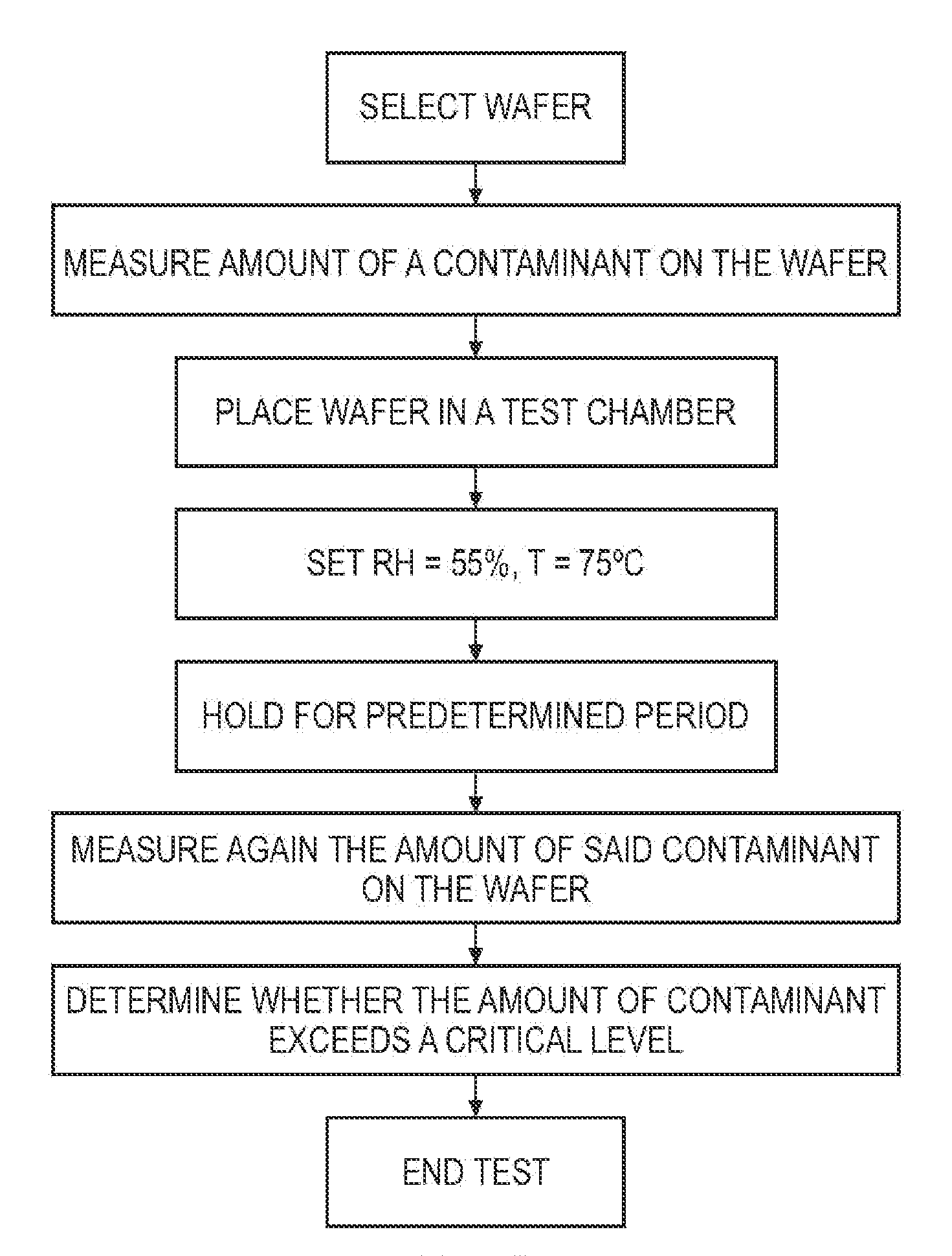
[0048]The SLAT test sequence begins with the selection of a wafer to be tested from a batch of wafers. The wafer is then inspected to determine an amount of contaminant present on one or more bondpads of the wafer.

[0049]According to the first embodiment, the wafer is subjected to Auger electron spectroscopy examination (AES) in order to determine a level of fluorine (F) contamination. In some embodiments the wafer is also subjected to SEM inspection to identify whether or not so-called white-dot defects are present. If white-dot defects are present, the number density of white-dot defects may be determined by inspection of an SEM image.

[0050]In some embodiments of the invention a thickness of any aluminum oxide or aluminum fluoride oxide is determined. In embodiments of the invention the thickness is determined using transmission electron microscopy (TEM).

[0051]The wafer to be tested is then mounted in a quartz holder and placed inside the test chamber. According to the present emb...

second embodiment

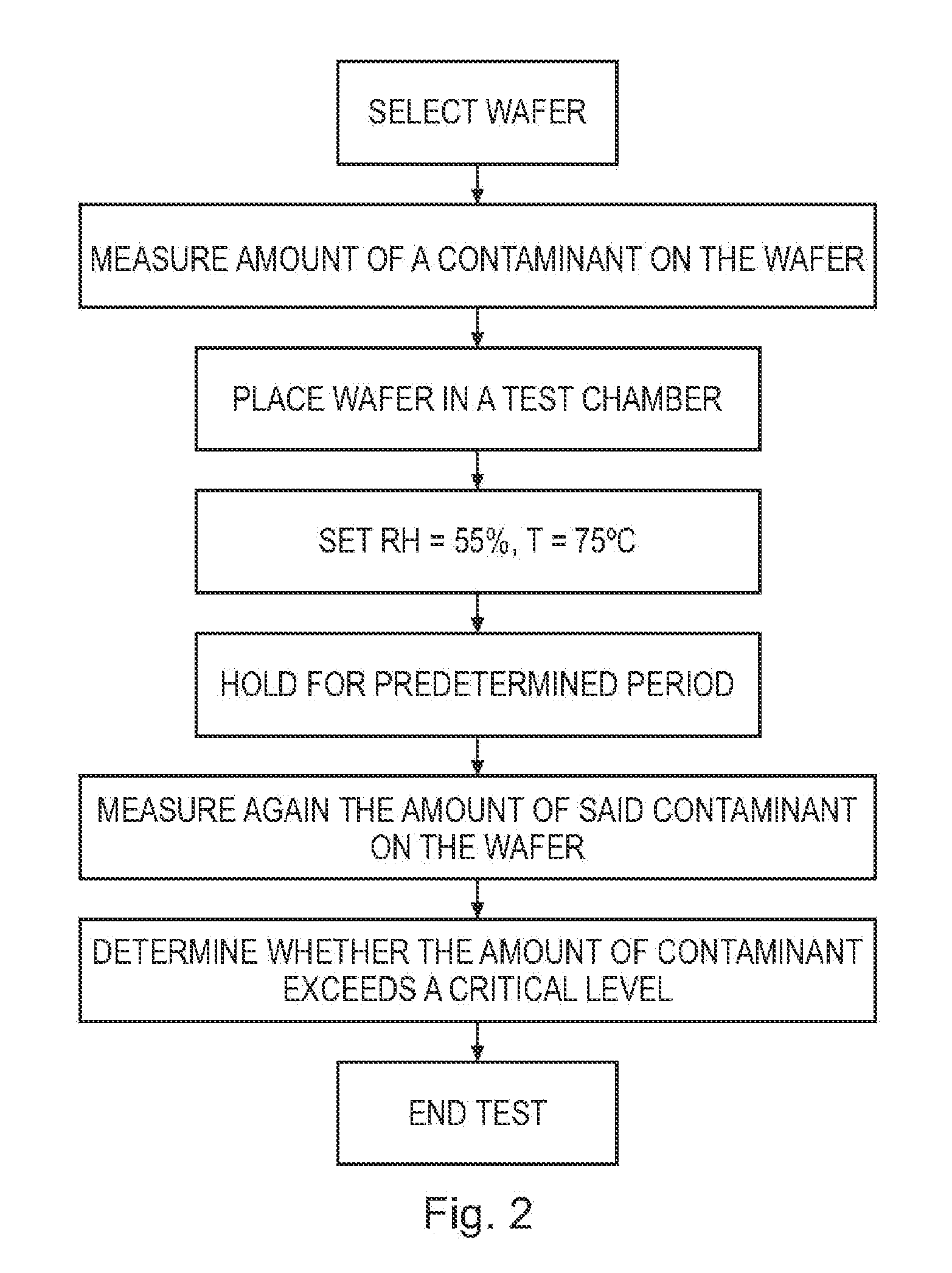
[0060]In the invention, a SLAT test is used to determine a maximum storage lifetime of a wafer.

[0061]FIG. 3. shows a flow diagram of a sequence of steps for the performance of a SLAT test according to the second embodiment.

[0062]As in the case of the first embodiment, the sequence of steps comprising the test begins with the selection of a wafer to be tested from a batch of wafers. The wafer is inspected to determine an amount of contaminants present on the wafer.

[0063]According to the second embodiment, the wafer is subjected to Auger electron spectroscopy examination (AES) in order to determine a level of fluorine (F) contamination. Other methods of determining a level of fluorine contamination are also useful.

[0064]It will be appreciated that the wafer may also be subjected to SEM inspection to identify whether or not so-called white-dot defects are present. If white-dot defects are present, the number density of white-dot defects may be determined by inspection of an SEM image.

[...


PUM

PropertyMeasurementUnit
temperatureaaaaaaaaaa

Abstract

Embodiments of the invention provide a method of determining a storage lifetime of a wafer in a storage environment, the storage environment corresponding to an environment having a first value of temperature and a first value of relative humidity, the wafer having a pre-test value of a first contamination parameter, including the steps of: subjecting the wafer to a test environment for a test period, the test environment includes an environment having a second value of temperature and a second value of relative humidity; subsequently, inspecting the wafer thereby to determine a post-test value of a second contamination parameter, wherein the second value of relative humidity is greater than 30% and the second value of wafer temperature is greater than 30° C.

Description

FIELD OF THE INVENTION[0001]The present invention relates to a method for performing shelf lifetime acceleration testing of integrated circuit (IC) wafers. In particular, but not exclusively, embodiments of the invention relate to a method of accelerating the testing of the shelf lifetime of an IC wafer by reference to the condition of bondpads of the IC.BACKGROUND OF THE INVENTION[0002]Integrated circuits typically comprise a large number of active and passive electronic devices formed on a single semiconductor wafer. Electrical connections (or ‘bonds’) between the wafer and external electrodes of (say) a wafer package are typically made by bonding ‘bondwires’ to ‘bondpads’ provided on the wafer.[0003]The problem exists that the surface of a bondpad can become contaminated. If the amount of contamination exceeds a critical value, bonds formed between a bondwire and a bondpad may be unreliable and susceptible to breakage. In some cases, if the amount of contamination is excessive, i...

Claims


Application Information

Patent Timeline
Patent Type & Authority Applications(United States)
IPC IPC(8): G01N17/00H01L21/66
CPCG01N17/006G01N2033/0095H01L24/85H01L2924/14H01L2224/85H01L2924/00014H01L2924/01019H01L2224/48H01L2224/45015H01L2924/207H01L2224/45099
Inventor ZHAO, SIPINGHUA, YOUNANNISTALA, RAMESH RAOLI, KUN
Owner CHARTERED SEMICONDUCTOR MANUFACTURING
Why Eureka
Try Eureka