Thin film transistor array panel and manufacturing method of the same
- Summary
- Abstract
- Description
- Claims
- Application Information
AI Technical Summary
Benefits of technology
Problems solved by technology
Method used
Image

Examples
exemplary embodiment 1
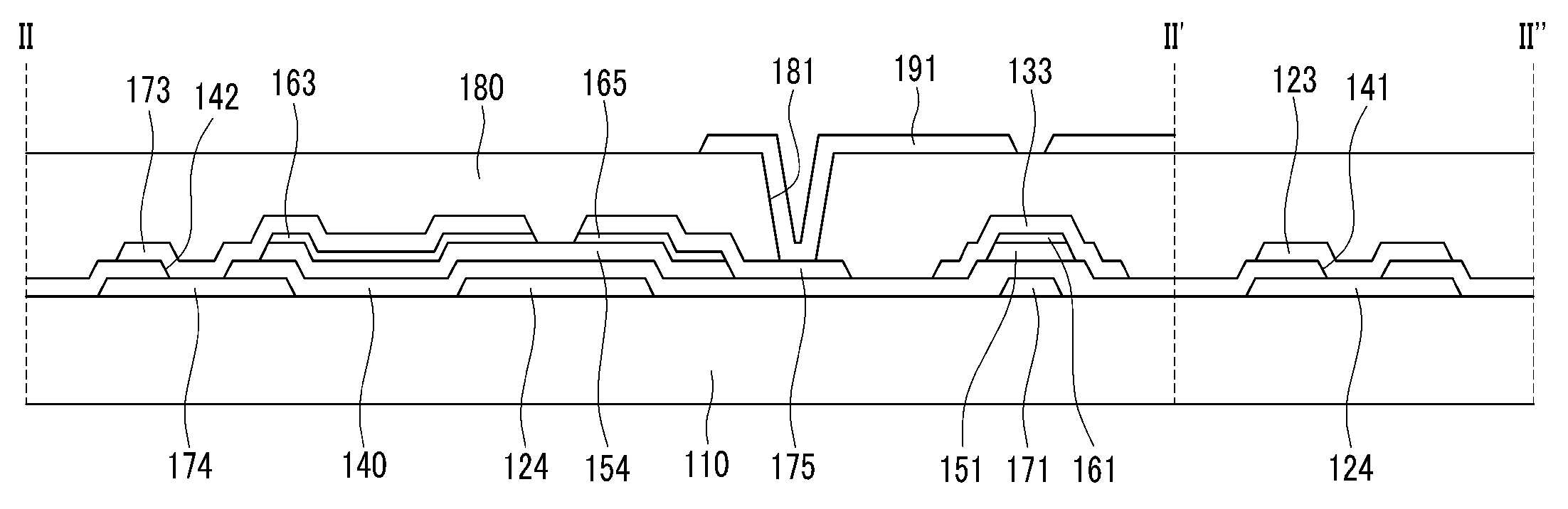
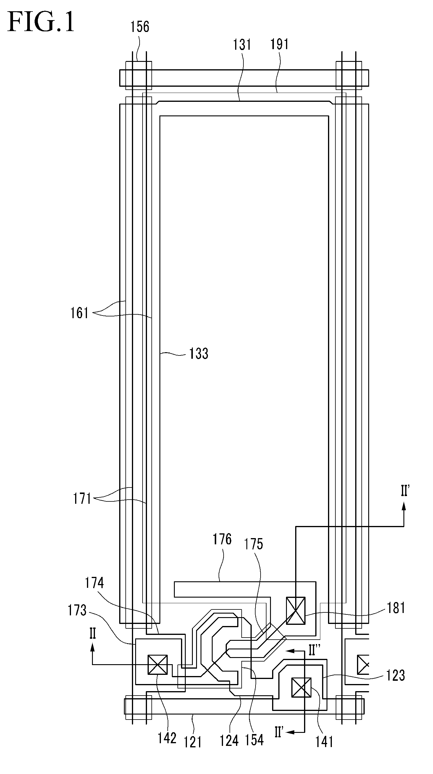
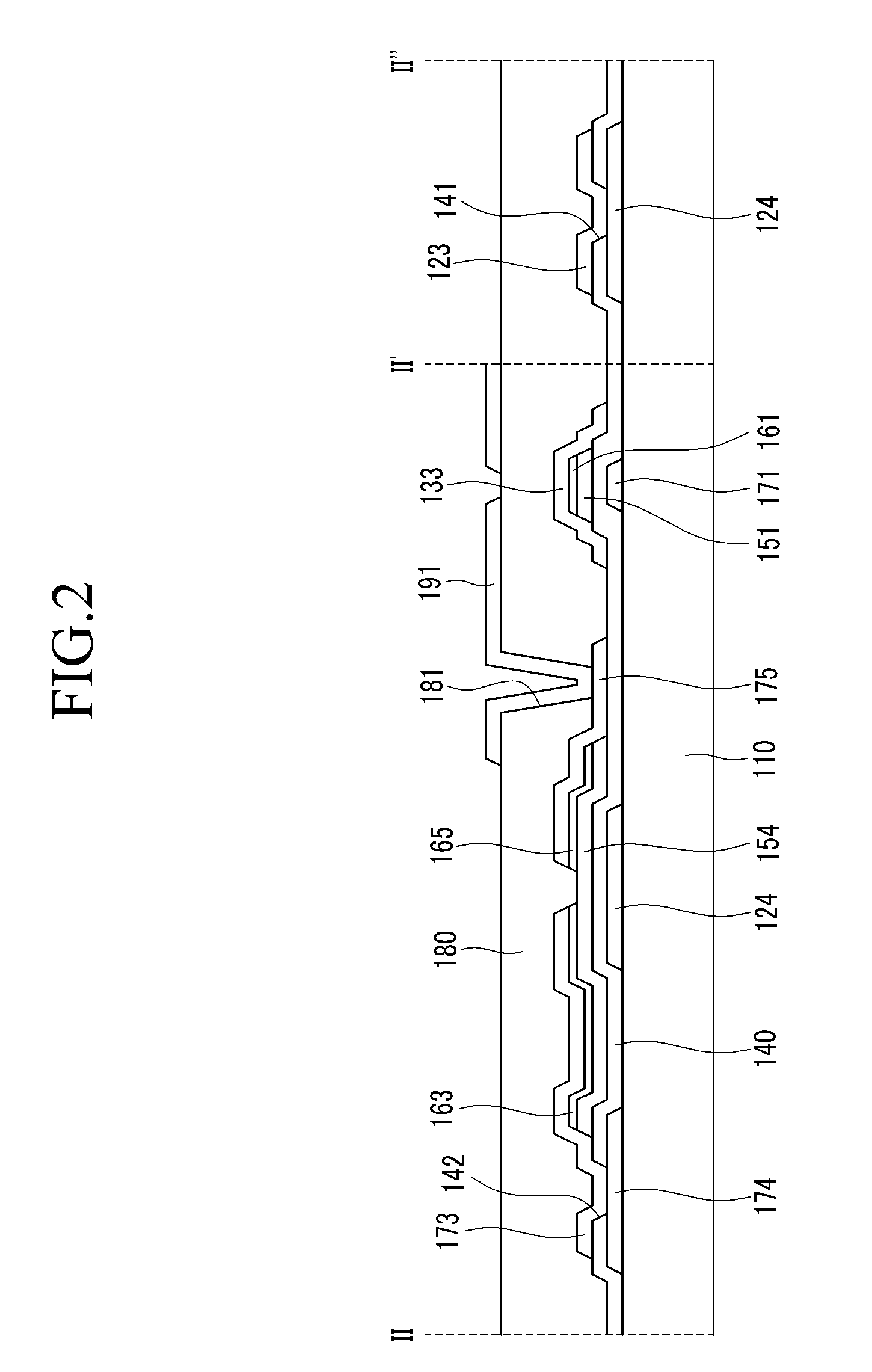
[0042]FIG. 1 is a plan view of an exemplary embodiment of a thin film transistor array panel, FIG. 2 is a cross-sectional view of the thin film transistor array panel shown in FIG. 1 taken along lines II-II′ and II′-II″, and FIG. 3 is an enlarged view of the thin film transistor in the thin film transistor array panel shown in FIG. 1.
[0043]A gate electrode 124 having an island shape and a data line 171 extending in a longitudinal direction are disposed on an insulating substrate 110, such as transparent glass. The data line 171 includes a plurality of expansions 174. The data line 171 transmits image signal voltages. The gate electrode 124 is disposed under a channel of the thin film transistor and includes a portion for applying the voltage and a portion for electrical connection to a gate line 121.
[0044]A gate insulating layer 140 is disposed on the gate electrode 124 and the data line 171. The gate insulating layer 140 has a contact hole 141 exposing the gate electrode 124 and a ...
exemplary embodiment 2
[0064]FIG. 14 is a plan view of an exemplary embodiment of a thin film transistor array panel, and FIG. 15 is a cross-sectional view along lines XV-XV′ and XV′-XV″ of FIG. 14.
[0065]The layered structure of the thin film transistor array panel shown in FIG. 14 and FIG. 15 is the same as that of the thin film transistor array panel shown in FIG. 1 and FIG. 2.
[0066]That is, a gate electrode 124 having an island shape and a data line 171 extending in a longitudinal direction are disposed on an insulating substrate 110 such as transparent glass. The data line 171 includes a plurality of expansions 174. A gate insulating layer 140 is formed on the gate electrode 124 and the data line 171.
[0067]The gate insulating layer 140 has a contact hole 141 exposing the gate electrode 124 and a contact hole 142 exposing the expansion 174 of the data line 171.
[0068]An intrinsic semiconductor 154, which may comprise amorphous silicon, is formed on the gate insulating layer 140.
[0069]Ohmic contacts 163 ...
PUM
 Abstract
Description
Claims
Application Information
 - Generate Ideas
- Intellectual Property
- Life Sciences
- Materials
- Tech Scout
- Unparalleled Data Quality
- Higher Quality Content
- 60% Fewer Hallucinations
Browse by: Latest US Patents, China's latest patents, Technical Efficacy Thesaurus, Application Domain, Technology Topic, Popular Technical Reports.
© 2025 PatSnap. All rights reserved.Legal|Privacy policy|Modern Slavery Act Transparency Statement|Sitemap|About US| Contact US: help@patsnap.com