Semiconductor digital circuit, FIFO buffer circuit, and data transferring method

a digital circuit and buffer circuit technology, applied in the direction of logic circuits, digital storage, pulse techniques, etc., can solve the problems of power consumption rising even more, and achieve the effect of easy layout design and design

Inactive Publication Date: 2009-11-12
NEC CORP
View PDF3 Cites 10 Cited by
  • Summary
  • Abstract
  • Description
  • Claims
  • Application Information

AI Technical Summary

Benefits of technology

[0030]As described above, in the semiconductor digital circuit of the present invention, it is possible to provide the boundary between areas operating at different power supply voltages at the same place as the boundary between areas operating at different clocks since the voltage level converting circuits are built into the FIFO buffer circuit, which becomes the boundary between areas operating at different clocks. More specifically, the two kinds of boundaries can be perfectly matched by building the voltage level converting circuits wherein the entry management flag circuits which include the boundary between areas operating at different clocks.
[0031]Further, in the semiconductor digital circuit of the present invention, since it is possible to match the boundary between areas operating at different power supply voltages with the boundary between areas operating at different clocks, the area where a single clock tree is formed becomes the same as the area where a single power supply network is formed in the layout design of the integrated circuit, making the design easy.
[0032]In other words, in the semiconductor digital circuit of the present invention, a small intermediate area is not necessary since the boundary between areas operating at different power supply voltages and the boundary between areas operating at different clocks can be matched by building the voltage level converting circuits into asynchronous or synchronous RS-FF circuits that manage entries by operating at the both clocks and that become the operation clock boundary in the FIFO buffer circuit and positioning the boundary between the areas operating at different power supply voltages at the same place as the boundary between the areas operating at different clocks.
[0033]Further, in the semiconductor digital circuit of the present invention, since the small area having a combination of a power supply voltage and a clock frequency different from those of the two areas is not necessary, the power supply wiring network and clock tree can be defined in the same circuit area and the layout design can be done easily.
[0034]In the present invention, by having the configuration and the operation as described above, in data transmission between two circuit areas having different combinations of a power supply voltage and an operation clock frequency, a voltage level conversion and a clock rate conversion can be performed at the same place at the same time.

Problems solved by technology

In recent years, as the number of elements formed on one chip of a semiconductor integrated circuit increases, the rise in power consumption has become even a bigger issue.

Method used


Image

  • Semiconductor digital circuit, FIFO buffer circuit, and data transferring method
  • Semiconductor digital circuit, FIFO buffer circuit, and data transferring method
  • Semiconductor digital circuit, FIFO buffer circuit, and data transferring method

Examples


example 1

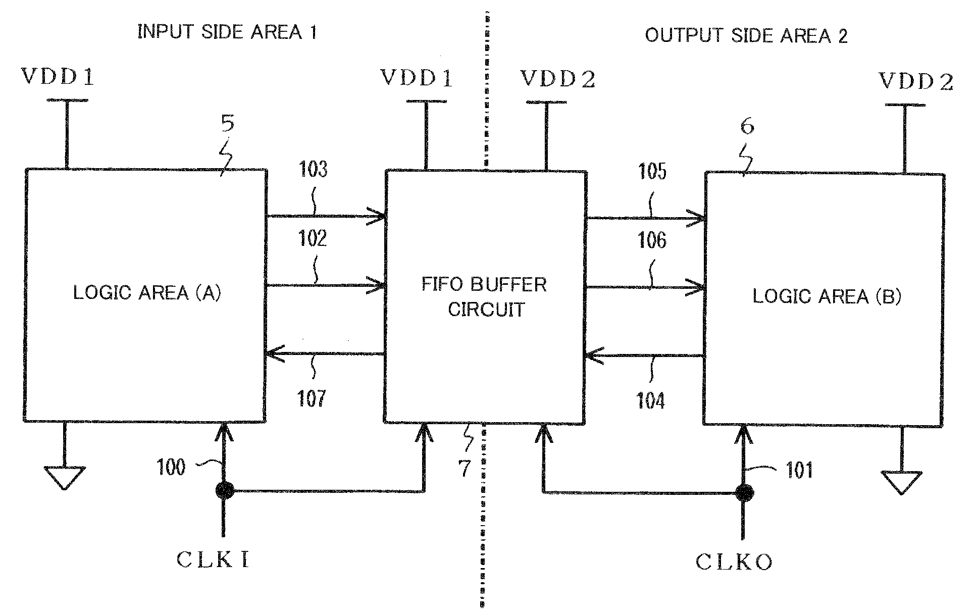
[0114]FIG. 3 is a drawing showing a configuration example of a data entry register of a FIFO buffer circuit according to a first example of the present invention. The configuration of the FIFO buffer circuit according to the first example of the present invention is the same as that of the FIFO buffer circuit according to the mode of the present invention shown in FIGS. 1 and 2, and the first example of the present invention will be described with reference to FIGS. 1 and 2 as well.

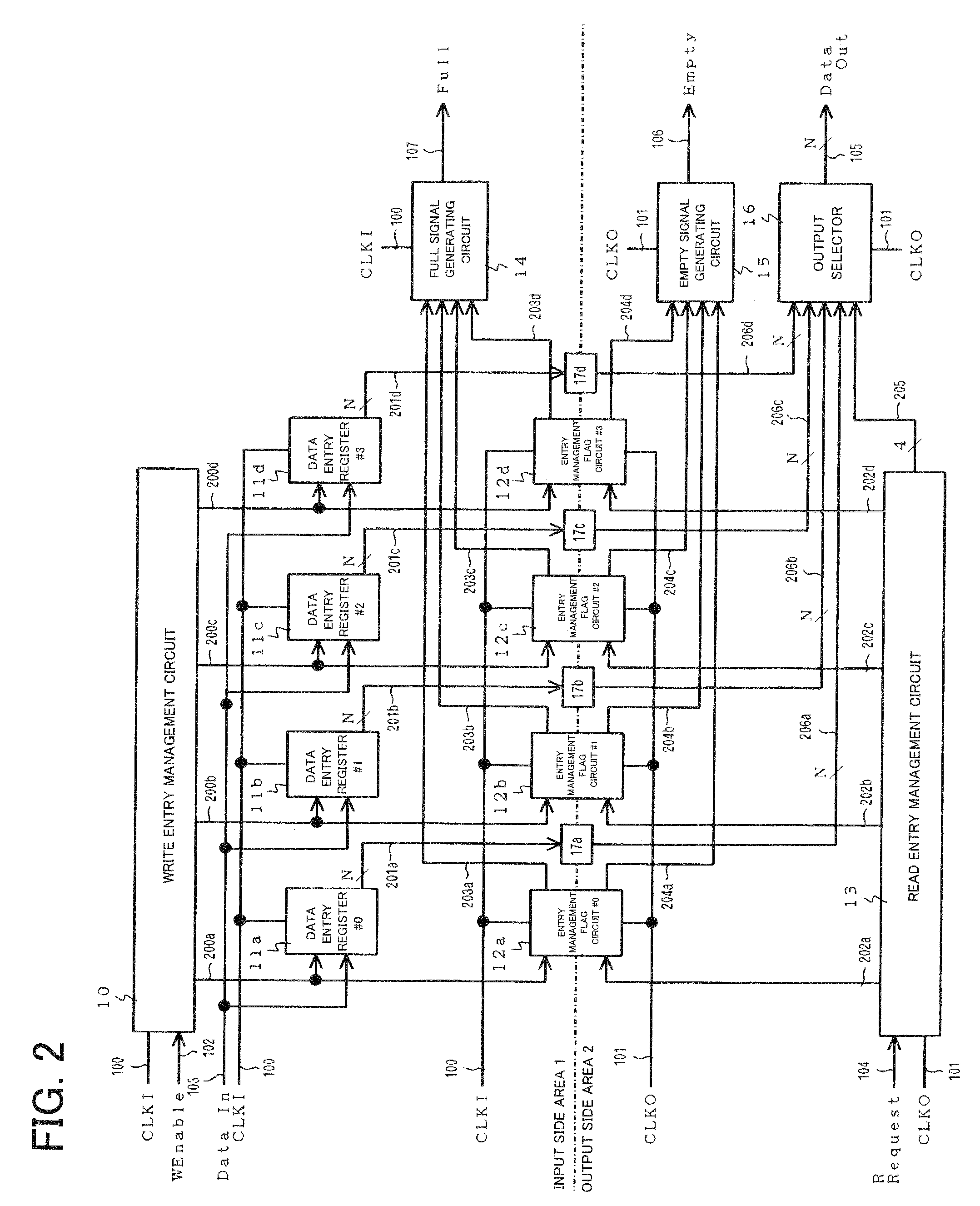
[0115]In FIG. 3, the data entry register 11 (the data entry registers 11a to 11d in FIG. 2) is constituted by disposing as many D-FF circuits 70a with an enable terminal as the bit number. The data input 103 is supplied to the input of each D-FF (D-Flip Flop) circuit 70a for each bit, and when D-FF circuit 70a receives an entry write signal 200, the data are written to the D-FF circuit 70a. The written data appear at an output 201 at the next clock. The write timing is determined by the input side area cl...

example 2

[0154]FIG. 15 is a drawing showing a configuration example of a full signal generating circuit of a FIFO buffer circuit according to a second example of the present invention. The configuration of the FIFO buffer circuit according to the second example of the present invention is the same as that of the FIFO buffer circuit according to the mode of the present invention shown in FIGS. 1 and 2, and the second example of the present invention will be described with reference to FIGS. 1 and 2. In FIG. 15, the full signal generating circuit is constituted by an inverter 52d, AND circuits 53g and 53h, an OR circuit 54d, D-FF circuits 71q and 71r, a pulse generator 22d, and an RS-FF circuit 23c.

[0155]As evident by the timing chart shown in FIG. 14, for instance, although the full signal 107 is temporarily generated within a clock cycle at timing T4, it is immediately cancelled since the data of the entry #0 is read. However, the timing of the cancellation is created by the read request si...

example 3

[0160]FIG. 17 is a drawing showing a configuration example when an RS-FF circuit 23b in an entry management flag circuit of an FIFO buffer circuit according to a third example of the present invention is constituted by CVSL circuits. The configuration of the FIFO buffer circuit according to the third example of the present invention is the same as that of the FIFO buffer circuit according to the mode of the present invention shown in FIGS. 1 and 2, and the third example of the present invention will be described with reference to FIGS. 1 and 2. In FIG. 17, the RS-FF circuit 23b is constituted by two loop-connected NOR circuits 51′ comprised of CVSL circuits.

[0161]In the RS-FF circuit 23b, a loop is formed by cross-connecting two NOR circuits 51′ comprised of CVSL circuits. One of the two NOR circuits 51′ comprised of CVSL circuits operates at the first power supply voltage VDD1 and the other operates at the second power supply voltage VDD2. Since the CVSL circuits also perform volta...


PUM


Abstract

A FIFO buffer circuit is provided which, in data transmission between two circuit areas having different combinations of a power supply voltage and an operation clock frequency, can perform a voltage level conversion and a clock rate conversion at the same place at the same time. In an input side area 1, there are disposed a plurality of data entry registers 11a-11d, a write entry management circuit 10 and a full signal generating circuit 14, while in an output side area 2, there are disposed a read entry management circuit 13, an empty signal generating circuit 15 and an output selector 16. On the boundary between the input and output side areas 1 and 2, there are disposed entry management flag circuits 12a-12d that manage the presence or absence of effective data in the respective data entries; and voltage level converting circuits 17a-17d that convert the voltage levels of the outputs of the data entry registers 11a-11d to the voltage levels of the output side. In this way, the clock rate replacements and voltage level conversions are performed.

Description

FIELD OF THE INVENTION[0001]The present invention relates to a semiconductor digital circuit, FIFO buffer circuit, and data transferring method, and particularly to a FIFO (First In First Out) buffer circuit that performs data transfer between two circuit areas having different power supply voltages and operation clocks.BACKGROUND OF THE INVENTION[0002]In recent years, as the number of elements formed on one chip of a semiconductor integrated circuit increases, the rise in power consumption has become even a bigger issue. In order to solve this problem, methods in which a circuit area is defined for a circuit block that realizes each function, and then the operation clock is stopped or is decreased the frequency for each of the circuit area, and the power supply voltage is lowered for each of the circuit area so as to reduce power consumption during operation are proposed. In these methods, the power supply voltage and the operation clock frequency might be different for each circui...

Claims


Application Information

Patent Timeline
Patent Type & Authority Applications(United States)
IPC IPC(8): H03K19/0175
CPCH03K19/0185
Inventor SUZUKI, KAZUMASA
Owner NEC CORP
Why Eureka
Try Eureka