High density package substrate and method for fabricating the same

a high density, substrate technology, applied in the direction of lithographic masks, etching metal masks, printed element electric connection formation, etc., can solve the problems of increased etching time, printed circuit boards, increased etching time, etc., and achieve high density and fine line capability.

Active Publication Date: 2009-11-19
NAN YA PRINTED CIRCUIT BOARD CORPORATION
View PDF2 Cites 27 Cited by
  • Summary
  • Abstract
  • Description
  • Claims
  • Application Information

AI Technical Summary

Benefits of technology

[0010]An object of the invention is to provide a high density package substrate and method for fabricating the same, which can prevent punch through caused by laser drilling and allow the substrate to have fine line capability.

Problems solved by technology

However, on the other hand, the thick copper foil increases etching time.
Therefore, increasing etching time worsens an undercut phenomenon of the printed circuit board and negatively affects the forming of fine lines.
However, the ultra-thin copper foil causes other problems, such as complicating the laser drilling process, increasing costs and increased probability of punch through.

Method used


Image

  • High density package substrate and method for fabricating the same
  • High density package substrate and method for fabricating the same
  • High density package substrate and method for fabricating the same

Examples


Embodiment Construction

[0016]The following description is of the best-contemplated mode of carrying out the invention. This description is made for the purpose of illustrating the general principles of the invention and should not be taken in a limiting sense. The scope of the invention is best determined by reference to the appended claims.

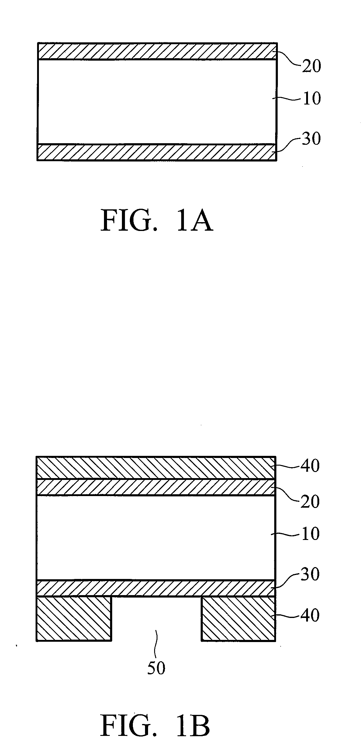
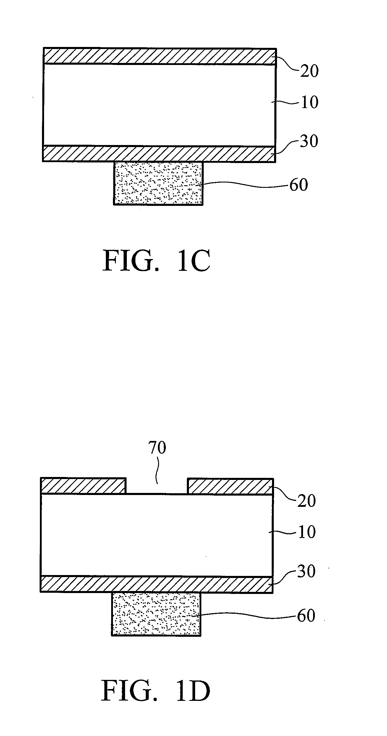
[0017]The following description of FIG. 1A to FIG. 1I is used to describe the fabrication method of a high density package substrate of the invention. The drawings are idealized representations for better illustration of the methods of the invention, and various elements are not necessarily shown to scale.

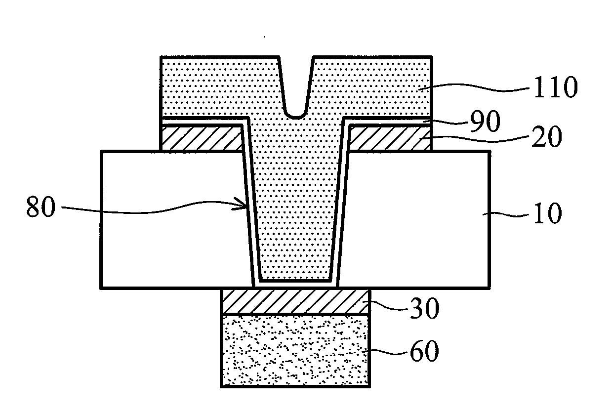
[0018]Referring to FIG. 1A, a double-sided copper clad laminate 10 having an upper copper foil 20 and a lower copper foil 30 is provided. The copper foil is an ultra-thin foil, with a thickness of about 4 μm or below. The double-sided copper clad laminate 10 comprises a core material of insulating materials, such as paper phenolic resin, composite epoxy, polyimide res...


PUM

PropertyMeasurementUnit
thicknessaaaaaaaaaa
thicknessaaaaaaaaaa
thicknessaaaaaaaaaa

Abstract

The invention provides a high density package substrate and a method for fabricating the same. A double-sided copper clad laminate containing an upper copper foil and a lower copper foil is provided. A bottom pad is disposed on the lower copper foil, aligned to a predetermined position of a through hole. The through hole is formed by laser drilling through the upper copper foil and the substrate, but not through the bottom pad. A seed layer is formed conformally lining the through hole, and a metal layer is formed on the seed layer by plating to form a plated through hole (PTH).

Description

CROSS REFERENCE TO RELATED APPLICATIONS[0001]This Application claims priority of Taiwan Patent Application No. 097118079, filed on May 16, 2008, the entirety of which is incorporated by reference herein.BACKGROUND OF THE INVENTION[0002]1. Field of the Invention[0003]The present invention relates to a high density package substrate and method for fabricating the same, and in particular relates to a method for forming a high density package substrate by laser drilling.[0004]2. Description of the Related Art[0005]Along with technological development, electrical devices are becoming lighter, thinner, shorter and smaller. As such, printed circuit boards in electrical devices are also being required to become lighter, thinner, shorter and smaller. Thus, high density interconnection (HDI) technology, allowing for high density interconnection, fine spacers and miniaturization, is being used in printed circuit boards to provide increased functions in a limited space and further decrease fabr...

Claims


Application Information

Patent Timeline
Patent Type & Authority Applications(United States)
IPC IPC(8): H05K3/42H05K1/02
CPCH05K3/0035H05K3/108H05K3/421Y10T29/49165H05K2201/0394H05K2201/09509H05K2203/0554H05K3/427
Inventor LEE, MENG-HANLAN, WEI-WENCHUANG, CHING-MINGSHANG, SHI-SHYAN JAMES
Owner NAN YA PRINTED CIRCUIT BOARD CORPORATION
Why Eureka
Try Eureka