
Multilayered lead frame for a semiconductor light-emitting device

a semiconductor and light-emitting device technology, applied in semiconductor devices, semiconductor/solid-state device details, electrical devices, etc., can solve the problems of low light reflectance and impair the and achieve the effect of efficient reflection of rear light and high luminous efficiency of the entire devi

Active Publication Date: 2009-11-19
PANASONIC HLDG CORP
View PDF11 Cites 0 Cited by
  • Summary
  • Abstract
  • Description
  • Claims
  • Application Information

AI Technical Summary

Benefits of technology

"The present invention provides a lead frame for a semiconductor device with improved light reflectance. The lead frame includes a lead frame body and a plurality of metal coatings that enhance light reflectance and wire bonding efficiency. The metal coatings may include a silver or silver-alloy coating, a gold or gold-alloy coating, a nickel or nickel-alloy coating, and a palladium or palladium-alloy coating. The lead frame also exhibits high light reflectance in the predetermined part, which improves the luminous efficiency of the entire device. The plurality of metal coatings may be applied in a predetermined order, and the lead frame may be used in a semiconductor light-emitting device."

Problems solved by technology

However, though this construction certainly has a high corrosion resistance, it has only a low light reflectance.
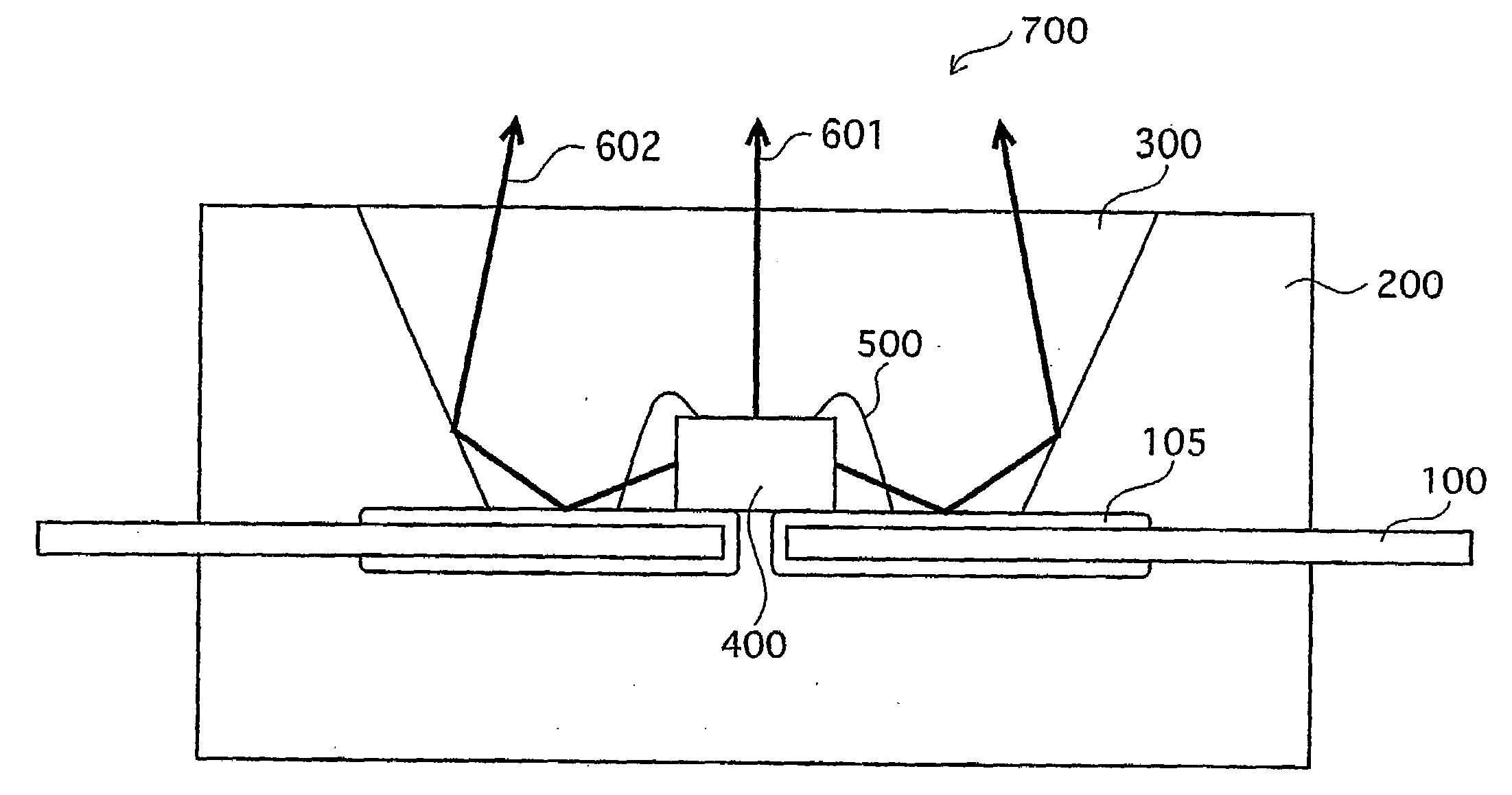
This being so, especially when a semiconductor light-emitting element such as an LED is mounted on the lead frame to form a semiconductor light-emitting device, the lead frame cannot sufficiently reflect rear light of the light-emitting element, which impairs the luminous efficiency of the entire device.

Method used


Image

  • Multilayered lead frame for a semiconductor light-emitting device
  • Multilayered lead frame for a semiconductor light-emitting device
  • Multilayered lead frame for a semiconductor light-emitting device

Examples


Embodiment Construction

[0032]An embodiment of the present invention is described in detail below, by referring to the drawings.

(Pattern of a Lead Frame)

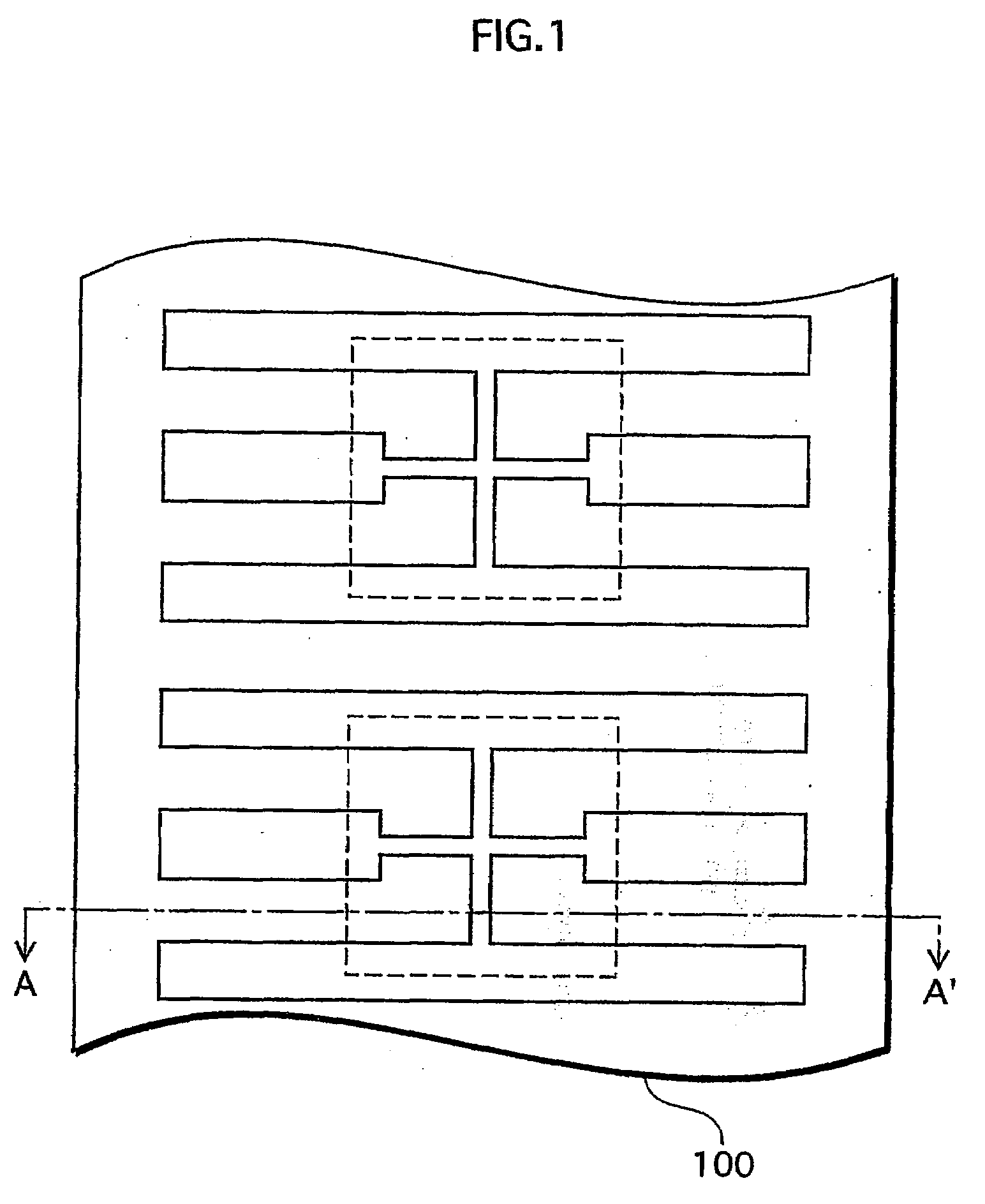
[0033]FIG. 1 is a top view of a lead frame to which the embodiment of the present invention relates.

[0034]In the drawing, a lead frame 100 is formed by pressing or etching a lead frame body in the illustrated pattern and then plating the lead frame body as described later. For example, the lead frame body is a thin plate of an iron alloy or a copper alloy.

[0035]A package for enclosing part of the lead frame 100 and housing a semiconductor element such as a semiconductor light-emitting element is provided in each of the areas indicated by the dashed line boxes. The package includes a base and a cover. The base has a depression for mounting the semiconductor light-emitting element. The cover seals the depression on which the semiconductor light-emitting element is mounted.

[0036]In this specification, a part of the lead frame 100 which is inside each of the a...


PUM


Abstract

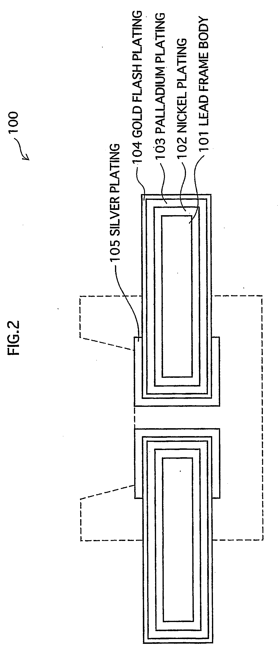
A lead frame (100) for a semiconductor device is formed by applying nickel plating (102), palladium plating (103), and gold flash plating (104) substantially entirely to lead frame body (101) such as copper thin plate in this order, and further applying silver plating (105) selectively to part of an inner part that is to be enclosed with a package of the semiconductor device. The lead frame (100) may also include a base of the package. The silver plating contributes to an excellent light reflectance and wire bonding efficiency of the inner part, whereas the gold flash plating contributes to an excellent resistance to corrosion and soldering efficiency of an outer part that is outside the package.

Description

RELATED APPLICATIONS[0001]This application is a Divisional of U.S. patent application Ser. No. 10 / 542,419, filed Dec. 29, 2005, which is a U.S. National Phase under 35 U.S.C. § 371 of International Application No. PCT / JP2004 / 000152, filed on Jan. 13, 2004, which in turn claims the benefit of Japanese Application No. 2003-007988, filed on Jan. 16, 2003, the entire contents of each of which are hereby incorporated by reference.TECHNICAL FIELD[0002]The present invention relates to a lead frame for a semiconductor device, and in particular relates to techniques of improving a light reflectance of a lead frame.BACKGROUND ART[0003]Conventionally, gold-silver alloy flash plating is formed at an outermost layer of a lead frame for a semiconductor device, to ensure a high resistance to corrosion. An example of such techniques is disclosed in Unexamined Japanese Patent Application Publication No. H11-008341.[0004]FIG. 6 is a representation of a construction of a lead frame described in the ab...

Claims


Application Information

Patent Timeline
Patent Type & Authority Applications(United States)
IPC IPC(8): H01L33/00H01L23/495H01L33/62
CPCH01L23/49582H01L33/62H01L2924/00014H01L24/48H01L2924/01079H01L2224/48091H01L2224/48247H01L2224/85439H01L2224/85464H01L2924/01046H01L2924/01078H01L2224/45099H01L2924/12041H01L2924/00H01L23/495
Inventor TOMOHIRO, HIDEKAZUFUJII, MASAYUKISATOU, NORIOYAMADA, TOMOYUKIKUSANO, TOMIO
Owner PANASONIC HLDG CORP
Learn More