

Display unit
a technology of display unit and display screen, which is applied in the direction of discharge tube/lamp details, discharge tube luminescnet screens, other domestic articles, etc., can solve the problems of non-uniformity of illumination, and achieve the effects of reducing leakage current through the organic layer, preventing the breaking of the second electrode, and large tilting angl
- Summary
- Abstract
- Description
- Claims
- Application Information
AI Technical Summary
Benefits of technology
Problems solved by technology
Method used
Image

Examples
first embodiment
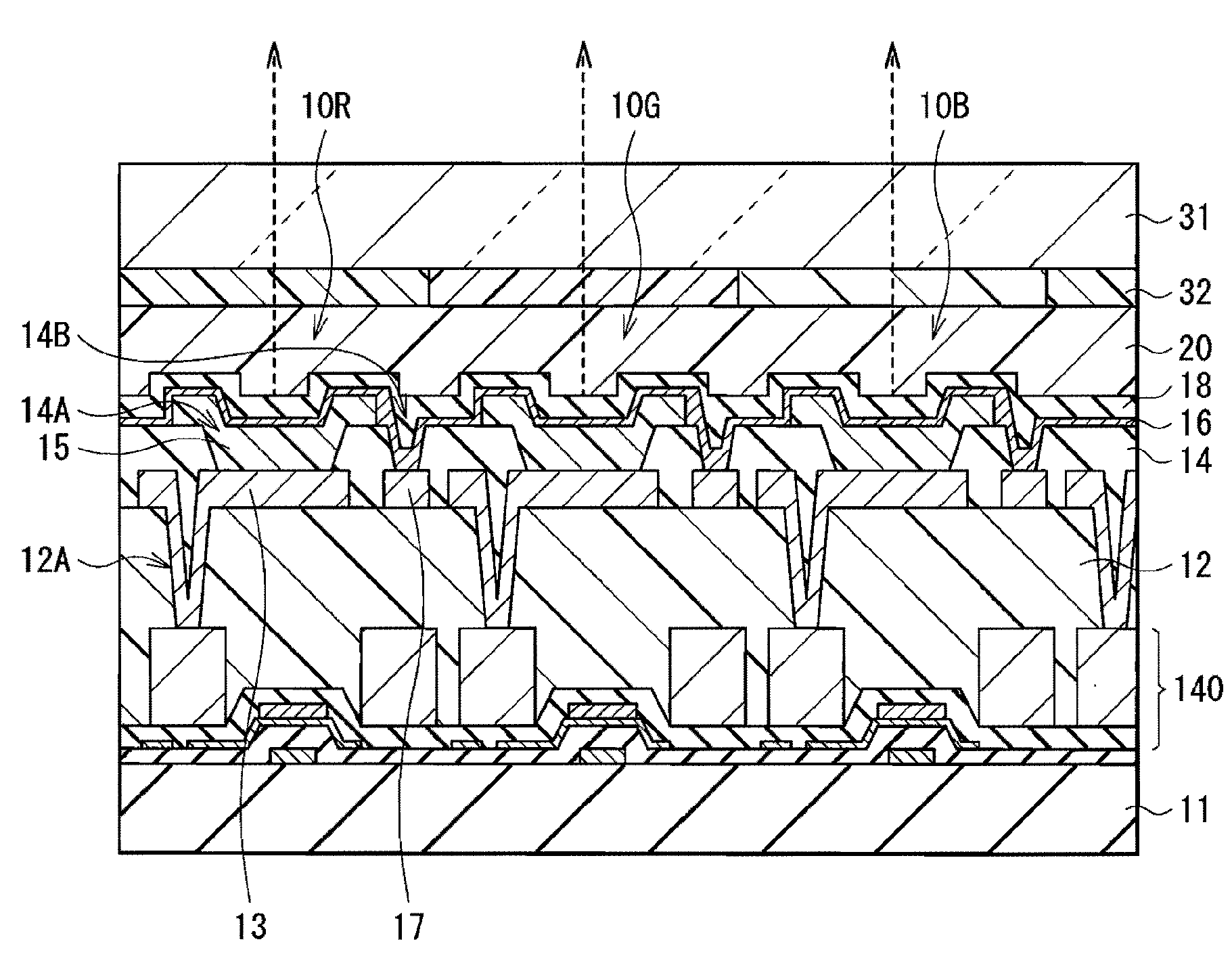
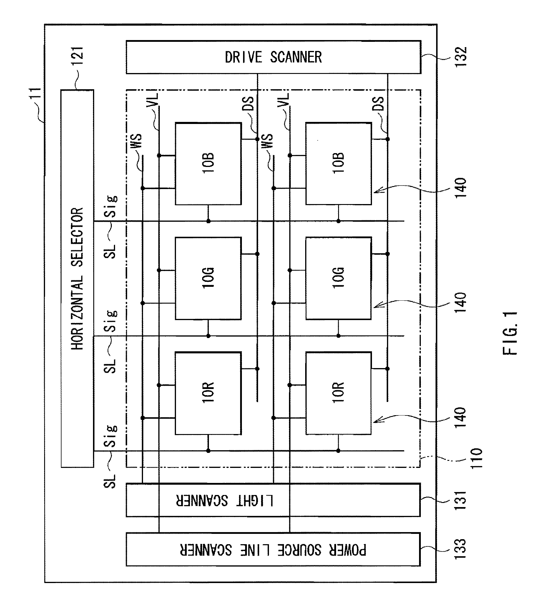
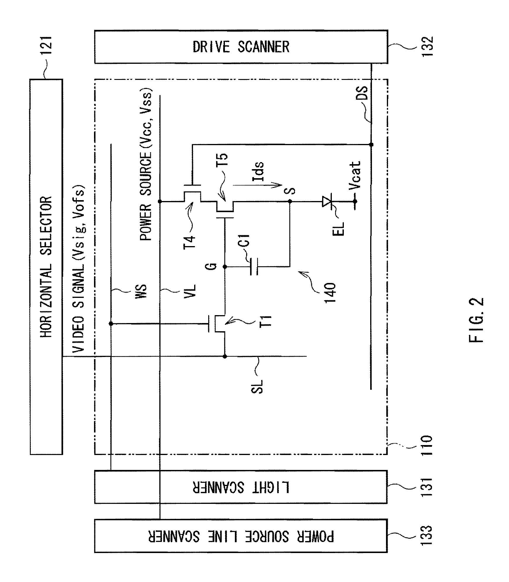
[0039]FIG. 1 illustrates a configuration of a display unit according to a first embodiment of the invention. The display unit is used as an ultrathin organic light emitting color display unit or the like. In the display unit, for example, a display region 110 in which a plurality of organic light emitting devices 10R, 10G, and 10B described later (hereinafter generically referred to as “organic light emitting device EL”) are arranged in a matrix state is formed on a substrate 11 made of glass, a silicon (Si) wafer, a resin or the like. On the periphery of the display region 110, a horizontal selector 121 as a signal section, and a light scanner 131, a drive scanner 132, and a power source line scanner 133 as a scanner section are formed.
[0040]In the display region 110, a plurality of signal lines SL are arranged in the column direction, and a plurality of scanning lines WS and DS and a plurality of power source lines VL are arranged in the row direction. A pixel circuit 140 includin...
second embodiment
[0082]FIG. 16 illustrates an example of a planar positional relationship of the insulating film 14 and the organic layer 15 of the display unit according to the second embodiment of the invention. FIG. 17 is a cross sectional structure taken along line XVII-XVII of FIG. 16. The display unit is configuration in the same manner as in the foregoing first embodiment except that the position of the low taper section 41 is different. Therefore, a description will be given by using the identical symbols for the corresponding elements.
[0083]This embodiment is suitable for a case in which the organic layer 15 is formed by transfer method. Specifically, the electron hole injection layer 15A, the electron hole transport layer 15B, and the electron transport layer 15D of the organic layer 15 are formed on the whole area by evaporation method, and the light emitting layer 15C is formed for the respective colors by transfer method. Thus, in a long side of the aperture 14A, an organic layer overla...
application examples
MODULE AND APPLICATION EXAMPLES
[0089]A description will be given of application examples of the display unit described in the foregoing embodiments. The display unit of the foregoing embodiments is applicable to a display unit of an electronic device in any field for displaying a video signal inputted from outside or a video signal generated inside as an image or a picture, such as a television device, a digital camera, a notebook personal computer, a portable terminal device such as a mobile phone, and a video camera.
Module
[0090]The display unit of the foregoing embodiments is incorporated in various electronic devices such as after-mentioned first to fifth application examples as a module as illustrated in FIG. 18, for example. In the module, for example, a region 210 exposed from a sealing substrate 50 and an adhesive layer 40 is provided in a side of the substrate 11, and an external connection terminal (not illustrated) is formed in the exposed region 210 by extending wirings o...
PUM
 Abstract
Description
Claims
Application Information