
Insulation film for capacitor element, capacitor element and semiconductor device

Inactive Publication Date: 2009-11-26
ELPIDA MEMORY INC
View PDF7 Cites 20 Cited by
  • Summary
  • Abstract
  • Description
  • Claims
  • Application Information

AI Technical Summary

Problems solved by technology

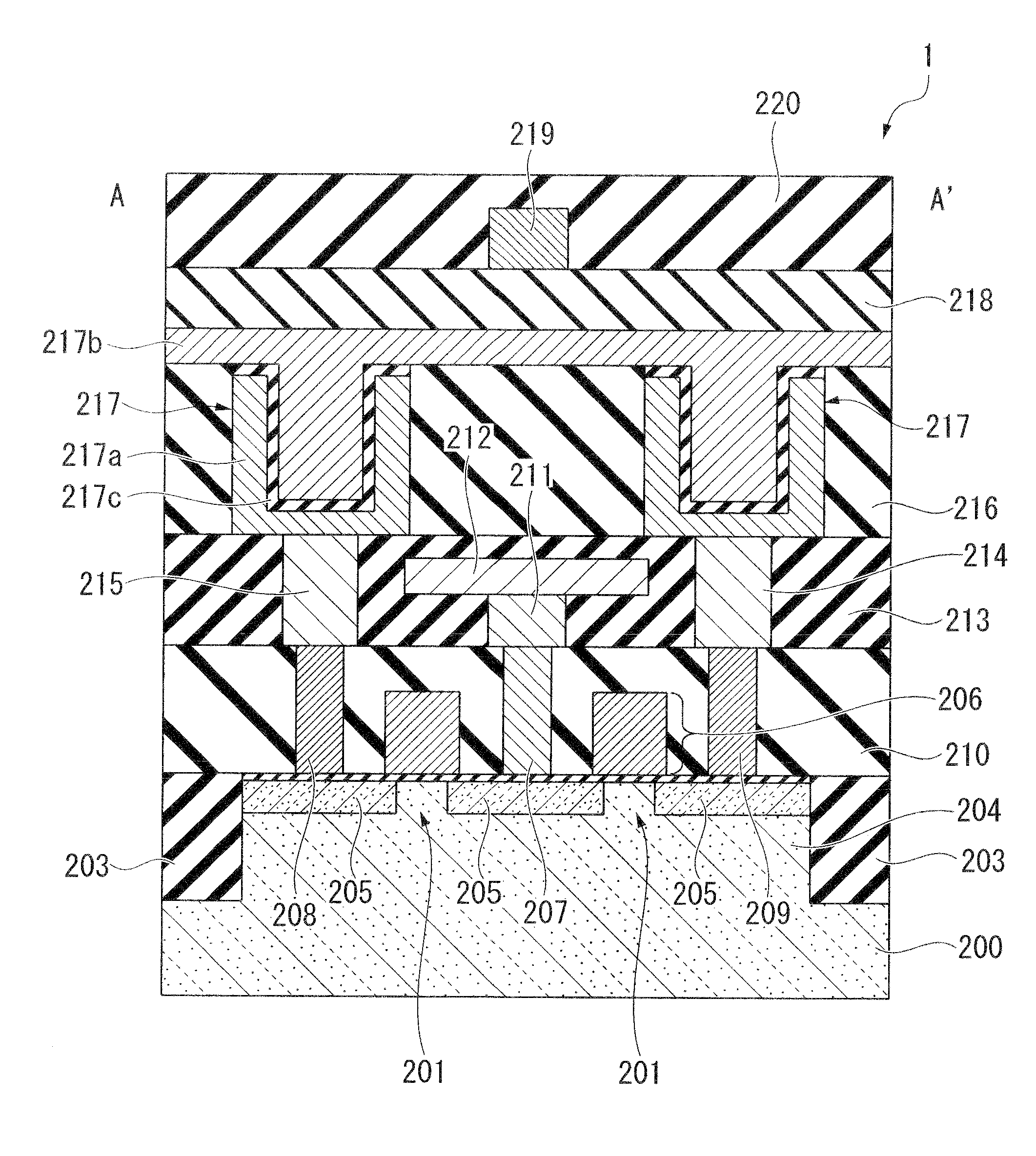
In conjunction with progress toward miniaturization and higher integration of DRAM, the size of the capacitor elements that configure memory cells has also contracted, thereby making it difficult to ensure a sufficient amount of stored charge.
Thus, while niobium pentoxide enables easy formation of film having high permittivity, inhibition of leakage current is difficult, and application to DRAM capacitor elements is problematic.
However, although Patent Document 1 discloses the heat treatment temperatures for formation of the insulation film, and evaluations of the permittivity of the insulation film, it discloses nothing regarding leakage current values of the insulation film.
However, it is extremely difficult to stably manufacture insulation film with this type of structure merely by temperature control.
That is, it is difficult to have amorphous material exist uniformly at all crystal grain boundary areas, with the result that it is difficult to form insulation film having the property of a uniform leakage current value regardless of location.

Method used


Image

  • Insulation film for capacitor element, capacitor element and semiconductor device
  • Insulation film for capacitor element, capacitor element and semiconductor device
  • Insulation film for capacitor element, capacitor element and semiconductor device

Examples


example 1

[0065]As example 1, an evaluation of the properties of a capacitor element which uses insulation film that is formed by adding yttrium to niobium pentoxide film is stated below.

[0066]First, the method of manufacture of the capacitor element used for evaluation is described As shown in FIG. 5, a silicon oxide film 11 (SiO2) was formed to a thickness of 50 nm by 1000° C. wet oxidation on top of a silicon substrate 10. Next, as a lower electrode, a platinum (Pt) film 12 was formed to a film thickness of 100 nm by the sputter method with DC discharge at 50 W power, at pressure of 1.0 Pa in an argon (Ar) gas atmosphere, and with the substrate temperature at room temperature.

[0067]Next, as insulation film 13, niobium pentoxide film was formed with addition of yttrium using a multi-source sputtering apparatus. During fabrication, RF discharges were simultaneously conducted inside the chamber of the sputtering apparatus using targets of Nb2O5 and Y2O3. Here, the semiconductor substrate 10 o...

example 2

[0072]As example 2, evaluation of the properties of a capacitor element which uses an insulation film that is formed by the addition of tantalum (Ta) to niobium pentoxide film is stated below.

[0073]With the exception of the insulation film, the capacitor element was formed by the same method as example 1, and platinum film was used as the lower electrode of the capacitor element. The insulation film was formed by the sputtering method, and Nb2O5 and Ta2O5 were used as the targets during film formation. The insulation film was subjected to annealing treatment for 10 minutes at 600° C. by a furnace apparatus using oxygen gas. After this annealing, the insulation film was in a state that was not completely crystallized. By controlling the RF power supplied to the respective targets, the addition ratio of tantalum relative to niobium (Ta / (Ta+Nb)) was varied in a range of 0-100%.

[0074]Table 1 shows the results of measurement of the ratio of tantalum and niobium in the formed insulation f...


PUM


Abstract

An insulation film includes niobium, oxygen and a metal element, and the insulation film has a band gap width of larger than 4.2 eV, and at least a portion of the insulation film includes an amorphous structure.

Description

BACKGROUND OF THE INVENTION[0001]1. Field of the Invention[0002]The present invention relates to an insulation film for a capacitor element, a capacitor element, and a semiconductor device.[0003]Priority is claimed on Japanese Patent Application No. 2008-134015, filed May 22, 2008, the content of which is incorporated herein by reference.[0004]2. Description of Related Art[0005]In conjunction with progress toward miniaturization and higher integration of DRAM, the size of the capacitor elements that configure memory cells has also contracted, thereby making it difficult to ensure a sufficient amount of stored charge. In order to ensure the amount of stored charge, development is progressing with respect to the application to capacitor elements of insulation film having high permittivity. As regards capacitor elements that configure DRAM memory cells, it is important not only to have high permittivity of the insulation film, but also to inhibit leakage current from the insulation fil...

Claims


Application Information

Patent Timeline
IPC IPC(8): H01L29/92H01G4/06E04B1/76
CPCH01G4/08H01G4/10H01L21/02175H01L21/02183H01L21/02192H01L28/91H01L21/02266H01L21/31604H01L27/10852H01L28/40H01L21/02194H10B12/033H01L21/0228
Inventor TANIOKU, MASAMI
Owner ELPIDA MEMORY INC
Learn More