
MECHANICALLY ROBUST METAL/LOW-k INTERCONNECTS

a technology of low-k interconnects and metals, applied in the direction of semiconductor devices, semiconductor/solid-state device details, electrical apparatus, etc., can solve the problems of reliability failure during thermo-, delamination during fabrication, and increase signal delays in ulsi electronic devices

Inactive Publication Date: 2009-12-03
GLOBALFOUNDRIES INC
View PDF10 Cites 45 Cited by
  • Summary
  • Abstract
  • Description
  • Claims
  • Application Information

AI Technical Summary

Benefits of technology

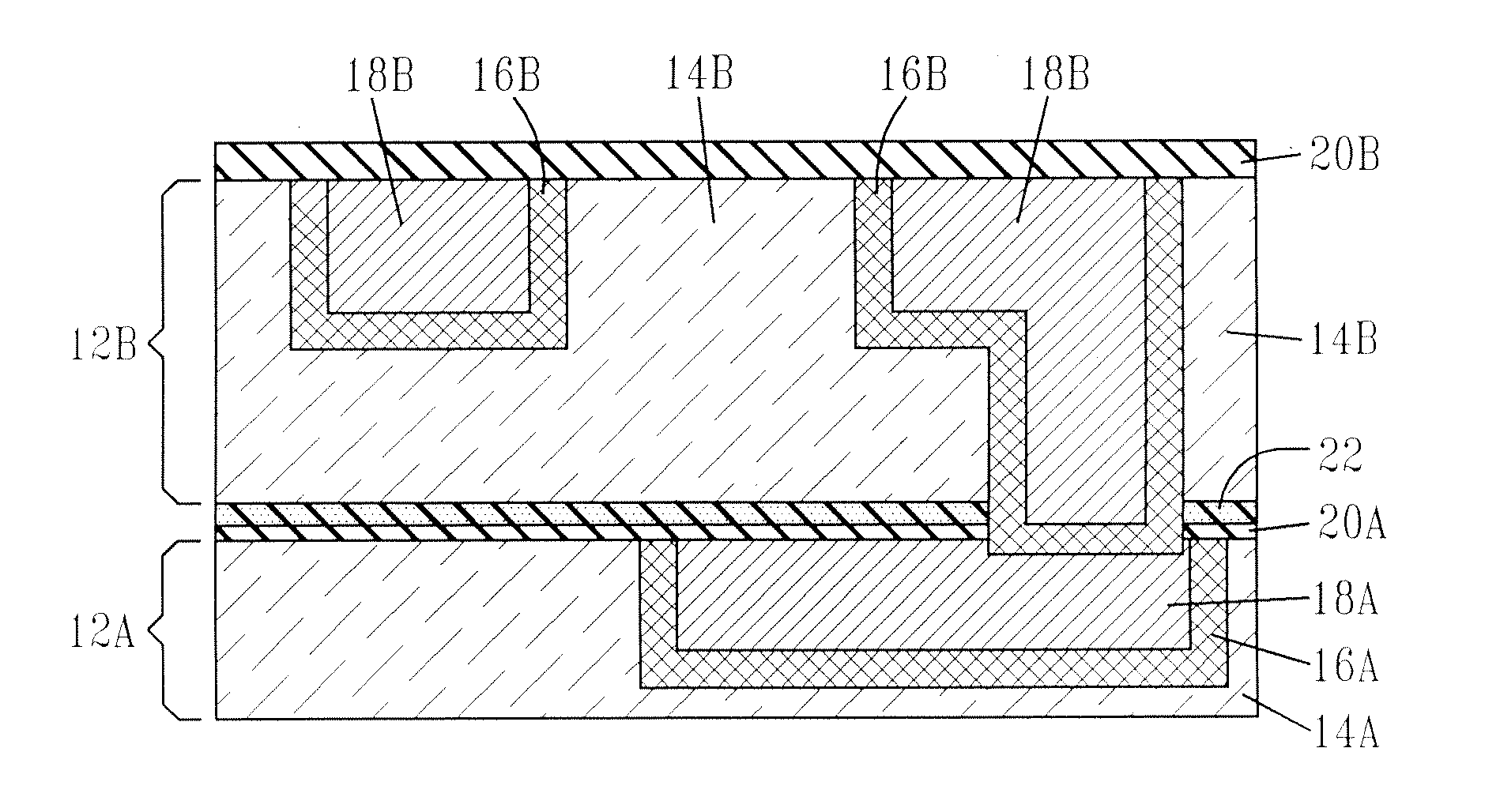
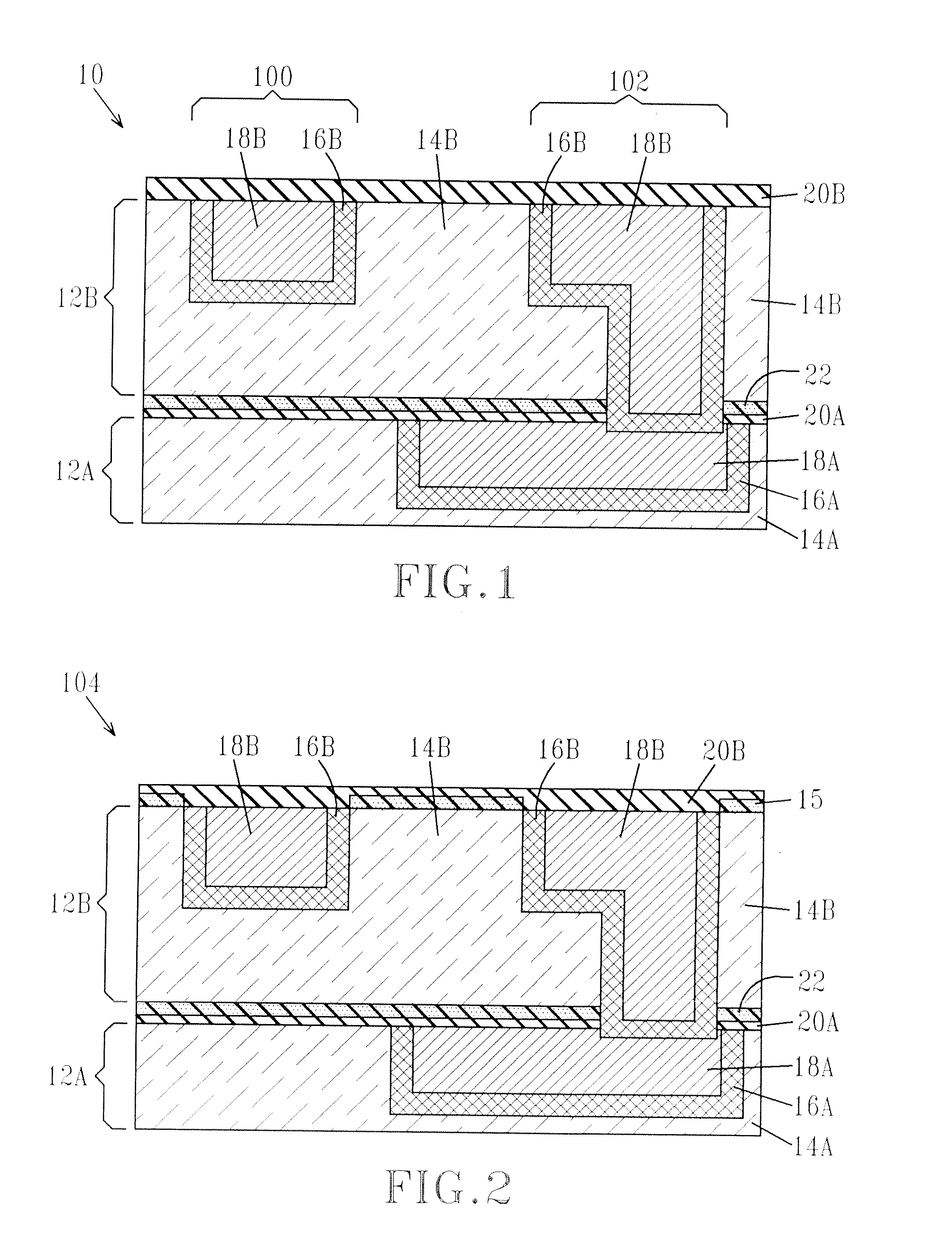
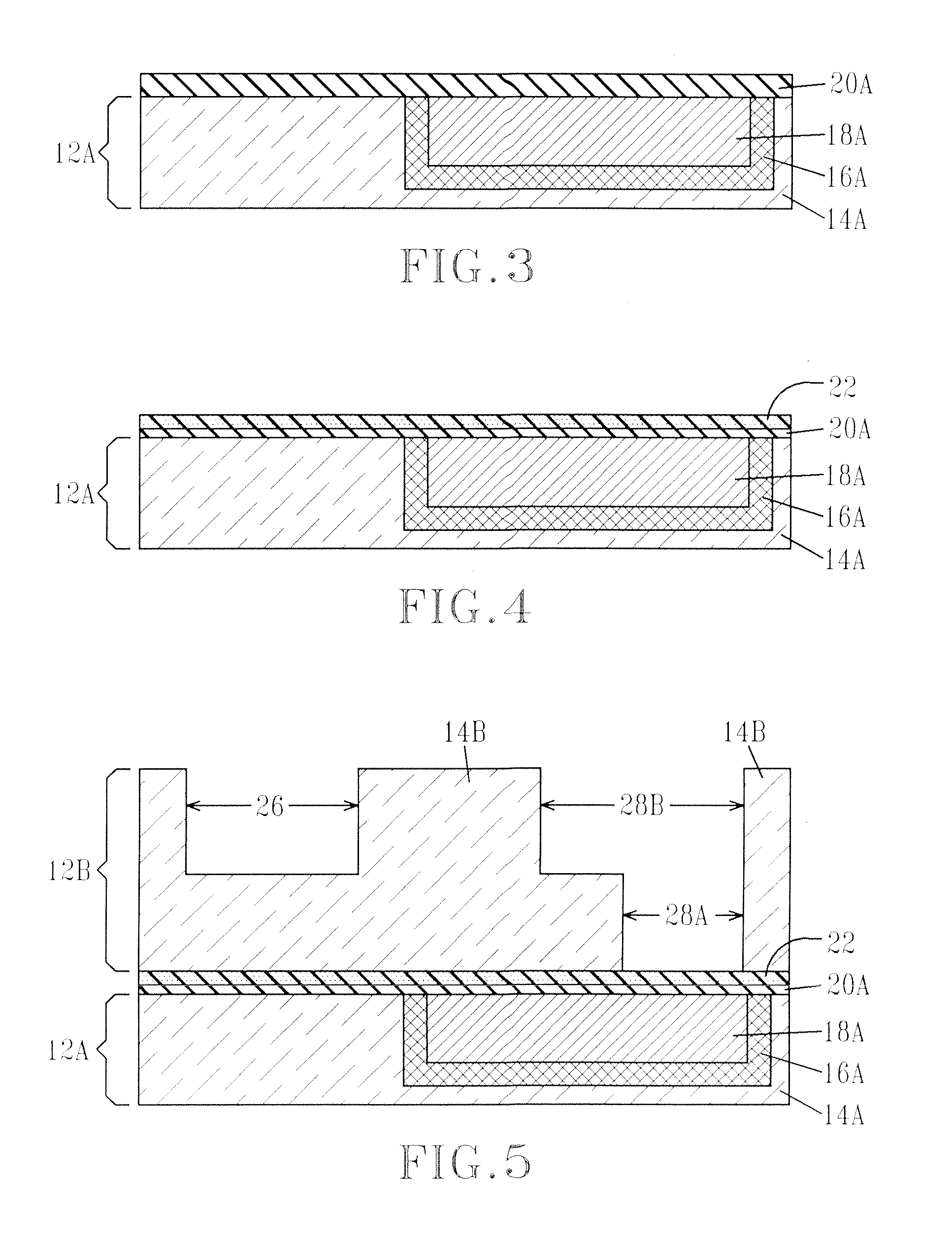
The present invention provides a mechanically robust insulating structure with improved adhesion strength between a low-k dielectric layer and a dielectric-containing substrate. This is achieved by treating the surface of the substrate with actinic radiation, plasma, electron beam radiation, or a combination thereof prior to low-k dielectric application. The invention also provides an electronic device structure incorporating layers of insulating and conductive materials as intralevel or interlevel dielectrics in a back-end-of-the-line wiring structure with enhanced adhesion strength between different dielectrics. The invention further provides a method for fabricating a mechanically robust interconnect structure with strong adhesion strength between the different layers.

Problems solved by technology

This combined effect increases signal delays in ULSI electronic devices.
The adhesion among the different layers in these complex structures is often too low, resulting in delamination during the fabrication of the device, and / or in response to thermo-mechanical stresses imposed by typical chip packaging materials, and / or reliability failure during thermo-mechanical stresses.
Weak interfaces in the interconnect structures can cause the delamination during fabrication and reliability failures during thermo-mechanical stress tests.
Despite the improved wettability and adhesion, the prior art wet treatment process disclosed in the aforementioned printed publication is limited to spin-on dielectric layers, which is not the mainstay of the state-of-the-art semiconductor manufacturing.
Moreover, the aforementioned technique addresses only the weak cohesive strength of the near-interface layer first deposited on the substrate, not the weak adhesion strength as encountered on porous low-k materials.
This prior method is limited to surface treatment of a conductive copper surface.
Again, this prior art method is limited to a surface treatment of the conductive copper surface for improving adhesion between copper and a dielectric layer deposited on top of the conductive copper layer.
This prior art method is limited to surface treatment of a low-k SOG interlayer dielectric (ILD) layer.
However adhesion improvement would only require ultra-thin layers, which would not be sufficient to alter etch selectivity.
However, this approach may not necessarily provide the requisite properties of the OSG film near the interface, in particular, adhesion and cohesive strength.
If an oxide-like layer is desired within the OSG film, there is no means provided to achieve that.

Method used


Image

  • MECHANICALLY ROBUST METAL/LOW-k INTERCONNECTS
  • MECHANICALLY ROBUST METAL/LOW-k INTERCONNECTS
  • MECHANICALLY ROBUST METAL/LOW-k INTERCONNECTS

Examples


example 1

Conventional; Not of the Invention

[0081]In this control example, a wafer containing an electronic structure having an upper layer of first dielectric with metal structures embedded in it was inserted in a plasma enhanced chemical vapor deposition (“PECVD”) reactor. The wafer was then heated to a temperature between room temperature and 350° C. In one example, Ar was flown into a 8″ the reactor at a rate of 30 scem to achieve a pressure of 100 mTorr. A high frequency RF power source connected to the substrate holder was then turned on to about 60.0 W for 0.5 to 2 minutes. In a different example, the RF power generated was operated under bias control at a bias of −250 VDC. Without interrupting the plasma, the precursor mixture used for the deposition of the next dielectric film i.e., a SiCNH capping layer, was then flown into the reactor keeping the power and pressure unchanged until the flow was stabilized an then for an additional 5-15 seconds. The Ar flow was then shut off and the ...

example 2

NH3 Plasma

[0083]In this inventive example, a wafer containing an electronic structure having an upper layer of first dielectric with metal structures embedded in it was inserted in a plasma enhanced chemical vapor deposition (“PECVD”) reactor. The wafer was then heated to a temperature between room temperature and 350° C. In one example, Ar was flown into a 8″ the reactor at a rate of 30 sccm to achieve a pressure of 100 mTorr. A high frequency RF power source connected to the substrate holder was then turned on to about 60.0 W for 0.5 to 2 minutes. In a different example, the RF power generated was operated under bias control at a bias of −250 VDC. Without interrupting the plasma, the precursor mixture used for the deposition of the next dielectric film (i.e., a SiCNH dielectric capping layer) was then flown into the reactor keeping the power and pressure unchanged until the flow was stabilized an then for an additional 5-15 seconds. The Ar flow was then shut off and the plasma con...

example 3

He Plasma

[0085]In this inventive example, a wafer containing an electronic structure having an upper layer of first dielectric with metal structures embedded in it was inserted in a plasma enhanced chemical vapor deposition (“PECVD”) reactor. The wafer was then heated to a temperature between room temperature and 350° C. In one example, Ar was flown into a 8″ the reactor at a rate of 30 sccm to achieve a pressure of 100 mTorr. A high frequency RF power source connected to the substrate holder was then turned on to about 60.0 W for 0.5 to 2 minutes. In a different example, the RF power generated was operated under bias control at a bias of −250 VDC. Without interrupting the plasma, the precursor mixture used for the deposition of the next dielectric film (i.e., a SiCNH dielectric capping layer) was then flown into the reactor keeping the power and pressure unchanged until the flow was stabilized an then for an additional 5-15 seconds. The Ar flow was then shut off and the plasma cond...


PUM

PropertyMeasurementUnit
dielectric constantaaaaaaaaaa
wavelengthaaaaaaaaaa

Abstract

A mechanically robust semiconductor structure with improved adhesion strength between a low-k dielectric layer and a dielectric-containing substrate is provided. In particular, the present invention provides a structure that includes a dielectric-containing substrate having an upper region including a treated surface layer which is chemically and physically different from the substrate; and a low-k dielectric material located on a the treated surface layer of the substrate. The treated surface layer and the low-k dielectric material form an interface that has an adhesion strength that is greater than 60% of the cohesive strength of the weaker material on either side of the interface. The treated surface is formed by treating the surface of the substrate with at least one of actinic radiation, a plasma and e-beam radiation prior to forming of the substrate the low-k dielectric material.

Description

CROSS-REFERENCE TO RELATED APPLICATIONS[0001]This application is a divisional of U.S. patent application Ser. No. 11 / 626,550, filed Jan. 24, 2007.BACKGROUND[0002]The present invention generally relates to a semiconductor electronic device structure comprising a low dielectric constant (i.e., low-k) dielectric having improved adhesion strength to a dielectric-containing substrate. The improved adhesion strength is achieved by treating the surface of the dielectric-containing substrate with at least one of actinic radiation, a plasma and electron beam radiation prior to the deposition of the low-k dielectric. Furthermore, the present invention relates to a method for improving the adhesion strength between different electrically conductive or dielectric layers including dielectrics that contain Si or C.[0003]The continuous shrinking in dimensions of electronic devices utilized in ultra-large scale semiconductor integrated (ULSI) circuits in recent years has resulted in increasing the ...

Claims


Application Information

Patent Timeline
Patent Type & Authority Applications(United States)
IPC IPC(8): H01L29/06
CPCH01L21/3105H01L21/76805H01L21/76834H01L21/76826H01L21/76825
Inventor LIN, QINGHUANGSPOONER, TERRY A.GANDHI, DARSHAN D.TYBERG, CHRISTY S.
Owner GLOBALFOUNDRIES INC
Learn More