

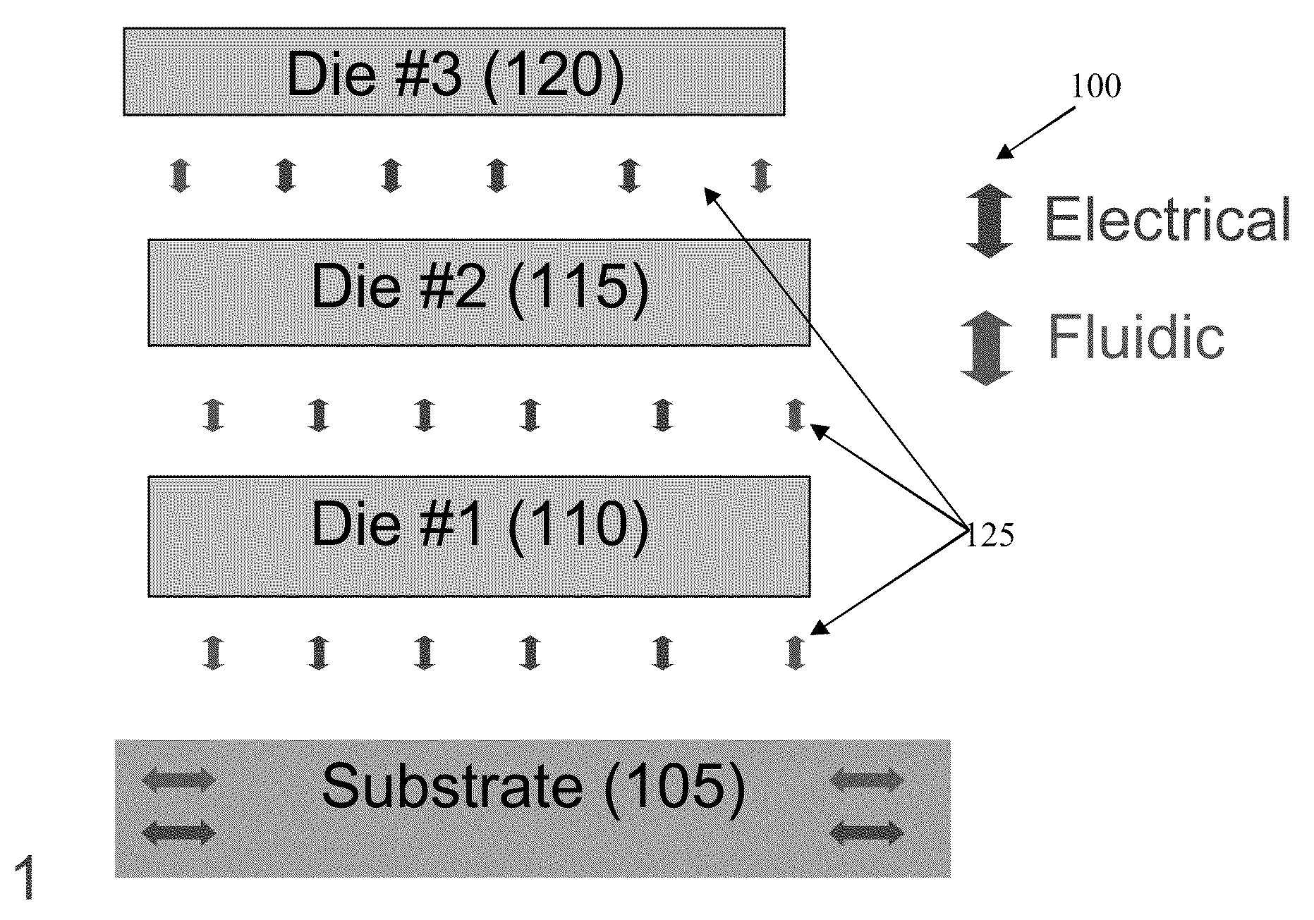
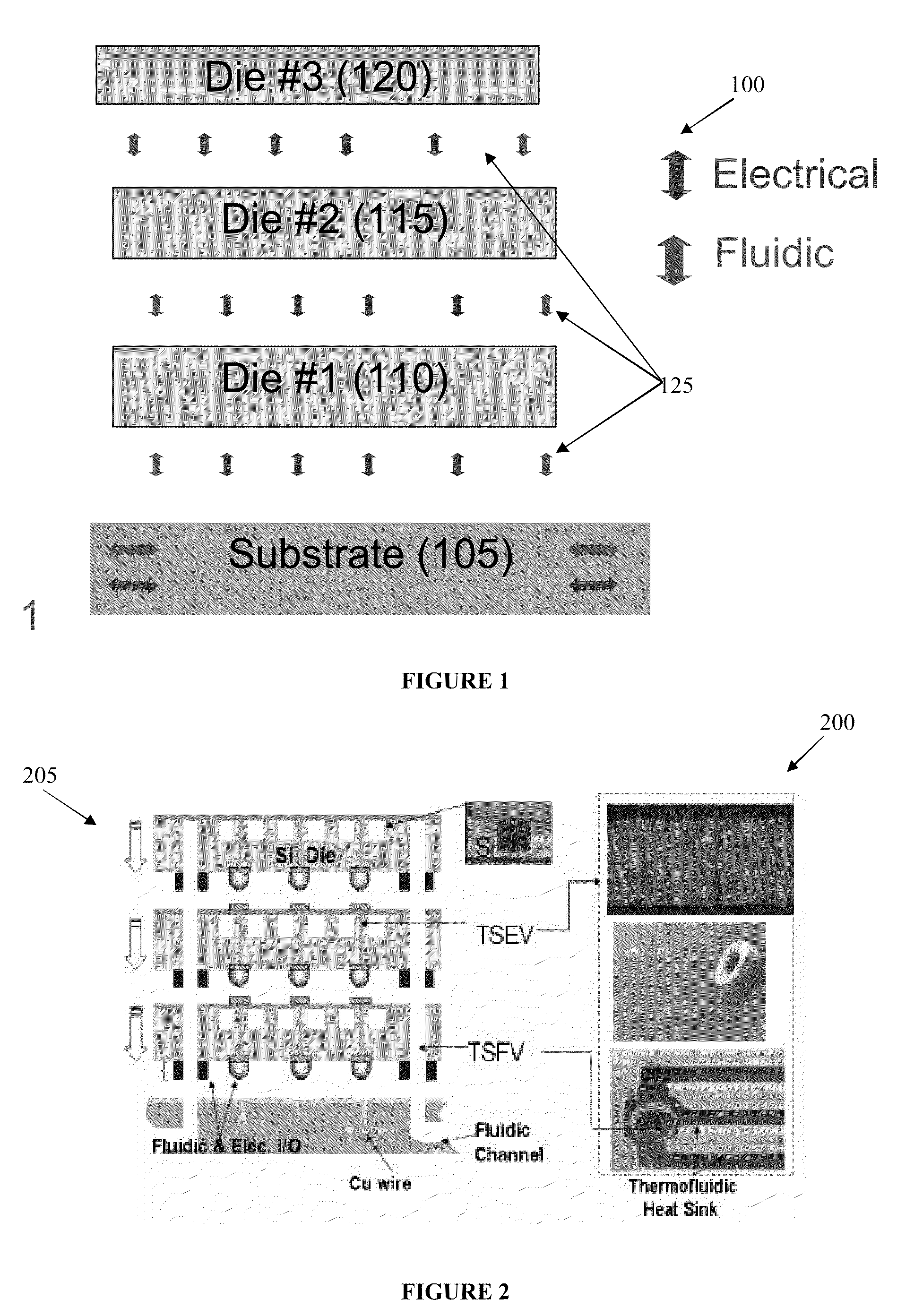
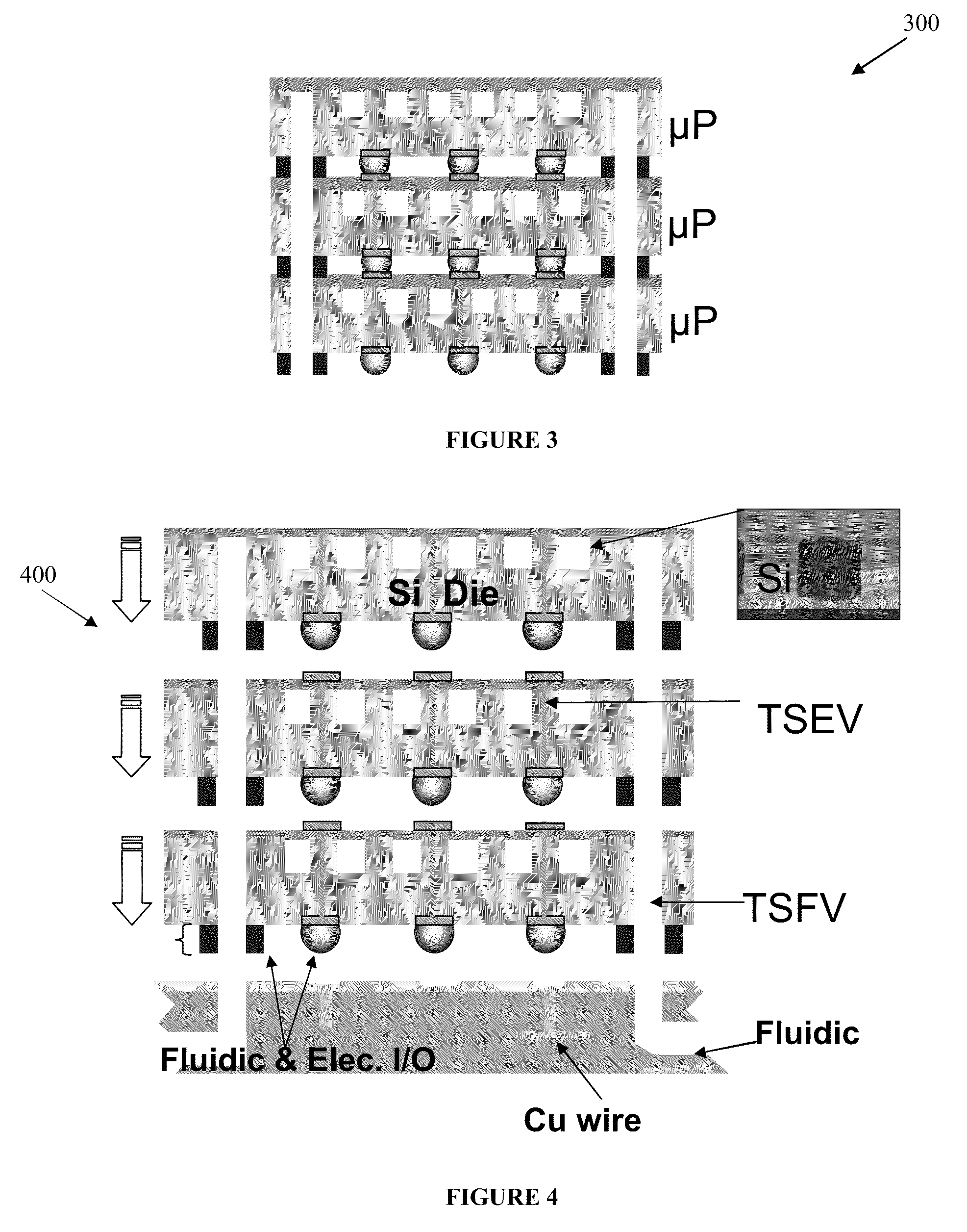
3-D ICs WITH MICROFLUIDIC INTERCONNECTS AND METHODS OF CONSTRUCTING SAME
a technology of microfluidic interconnects and integrated circuits, applied in the field of three-dimensional integrated circuits, can solve the problems of reducing device hot spots, affecting device operation, affecting end user usage patterns, etc., and achieve the effect of preventing the absorption of coolant by wafers
- Summary
- Abstract
- Description
- Claims
- Application Information
AI Technical Summary
Benefits of technology
Problems solved by technology
Method used
Image

Examples
Embodiment Construction
[0027]The International Technology Roadmap for Semiconductors (ITRS) projects that power dissipation will reach 151 W and 198 W for cost performance and high-performance applications, respectively, by 2018 at the 18 nm technology node. Consequently, it is not likely that conventional heat removal techniques will meet the power density, heat flux, and thermal resistance needs of future high performance microprocessors.
[0028]Liquid cooling using microchannels, as discussed herein, can meet the thermal management requirements of high-performance microprocessors due to high heat transfer coefficient. Although a number of researchers have explored advantages of using liquid cooling to mitigate future thermal management problems, heretofore many unknowns existed for implementation, especially for 3-D integrated systems. These unknowns include fabrication of an on-chip microfluidic heat sink and integration of electrical through-silicon vias (TSVs), where to place fluidic I / O interconnects...
PUM
 Abstract
Description
Claims
Application Information