Semiconductor device

a semiconductor device and semiconductor technology, applied in the field of semiconductor devices, can solve the problems of erroneous operation of semiconductor devices, inability to transmit signals, waveform distortion, etc., and achieve the effects of reducing impedance, low capacitance, and reducing waveform distortion

Inactive Publication Date: 2009-12-03
PANASONIC CORP
View PDF7 Cites 7 Cited by
  • Summary
  • Abstract
  • Description
  • Claims
  • Application Information

AI Technical Summary

Benefits of technology

[0013]With this configuration, the signal of the semiconductor element is directly transmitted to the first signal pad via the signal through via without passing through wires on the first substrate. Thus, it is possible to realize a low-resistance, low-capacitance transmission line, and to reduce the waveform distortion by the RC time constant.
[0014]The semiconductor element further includes: a second ground pad formed on the upper face and connected to the first ground pad; a second power supply pad formed on the upper face and connected to the first power supply pad; a ground through via running through the second substrate and connected to the second ground pad; and a power supply through via running through the second substrate and connected to the second power supply pad. Thus, it is possible to reduce the impedance against the supply of the power supply voltage and the ground voltage, and to reduce simultaneous switching noise, etc., entailing a high-speed operation.
[0015]As described above, with the semiconductor device of the present invention, the high-speed transfer interface signal of the semiconductor element can be transmitted to the signal pad on the carrier via the signal through via and the signal pad without the signal passing through wires on the first substrate. Thus, it is possible to reduce the signal waveform distortion by the RC time constant.

Problems solved by technology

In such a case, however, the following problems may arise.
First, the signal of the interface terminal of the second semiconductor element, which handles a high-speed signal such as DDR, DDR2, DDR3 or LVDS, also propagates through the wiring portion on the underlying first semiconductor element or the silicon interposer, and the “RC time constant” between the wire resistance on the second semiconductor and the capacitance with respect to the Si substrate may cause a waveform distortion, whereby it is not possible to transmit the signal at a signal transfer rate as defined by the standard.
This may lead to an erroneous operation of the semiconductor device, and hence the electronic apparatus.
Therefore, there is possibly a voltage drop due to the wire resistance or switching noise due to the inductance, and the logic element may operate erroneously due to the disturbance in the signal transfer or the disturbance in the power supply potential or the ground potential.
This may lead to an erroneous operation of the semiconductor device, and hence the electronic apparatus.

Method used


Image

  • Semiconductor device
  • Semiconductor device
  • Semiconductor device

Examples


first embodiment

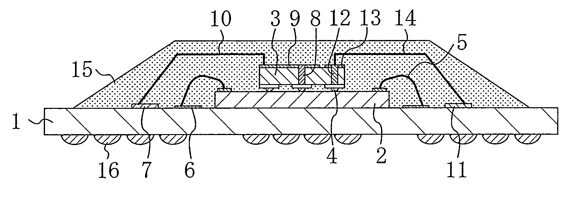
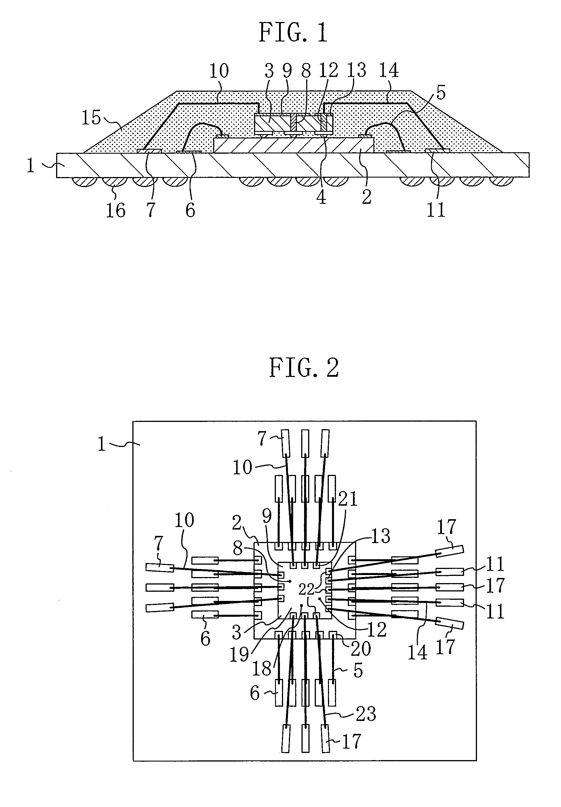
[0022]FIG. 1 is a cross-sectional view schematically showing a semiconductor device according to a first embodiment of the present invention, and FIG. 2 is a plan view showing the semiconductor device of the first embodiment as viewed from above. The mold resin is not shown in FIG. 2 for a better understanding of the structure.

[0023]As shown in FIGS. 1 and 2, the semiconductor device of the present embodiment includes a BGA substrate 1, a first semiconductor element 2, and a second semiconductor element 3. The BGA substrate 1 includes signal pads 6 and 11, GND pads 17 and power supply pads 7 formed on its upper face, and metal balls 16 formed on its reverse face. The first semiconductor element 2 is mounted on the upper face of the BGA substrate 1 with its circuit formation face facing up, and with signal pads 20 formed on its upper face (circuit formation face). The second semiconductor element 3 is mounted on the upper face of the first semiconductor element 2 with its circuit for...

second embodiment

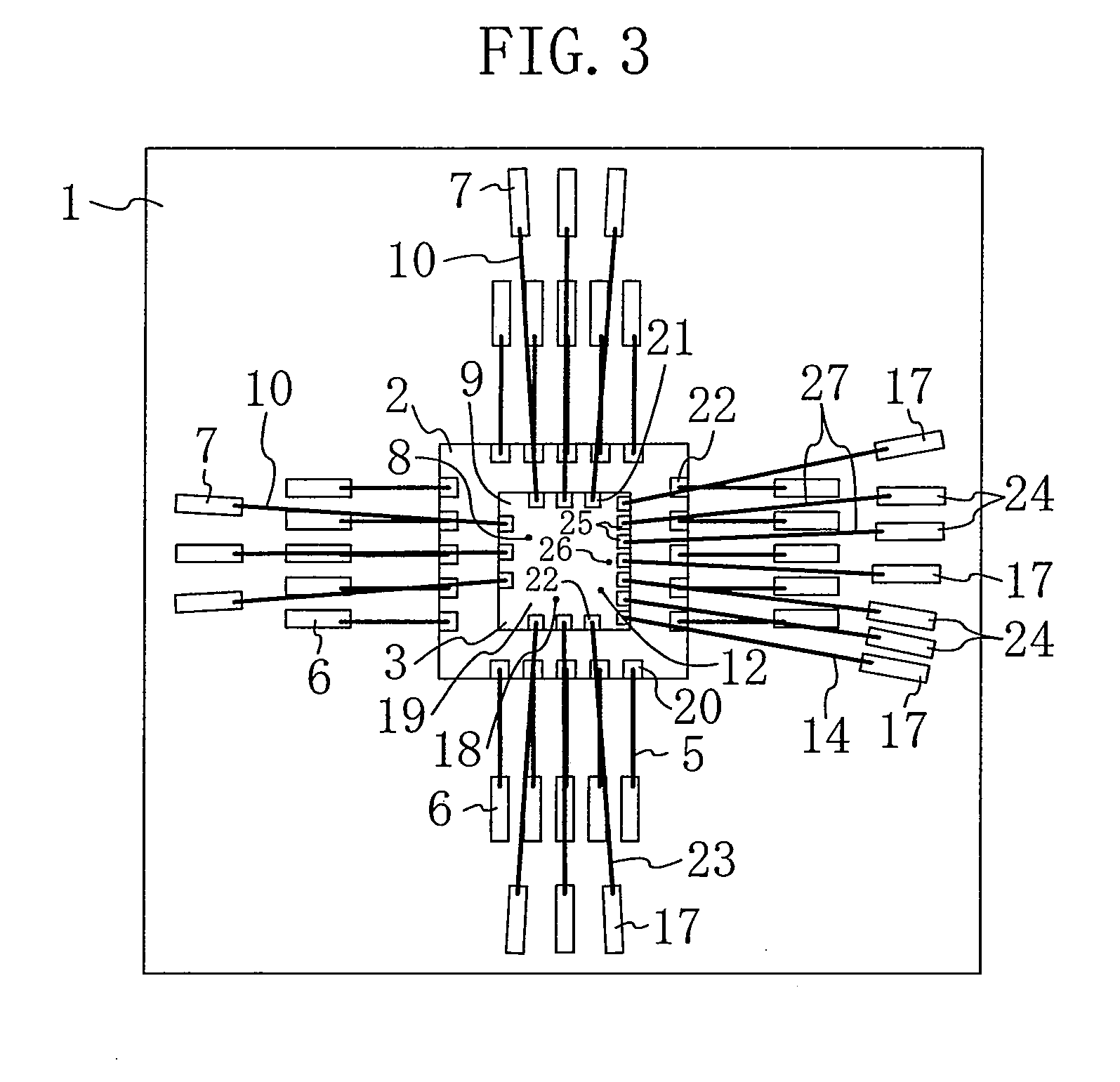
[0038]FIG. 3 is a plan view showing a semiconductor device according to a second embodiment of the present invention as viewed from above. In FIG. 3, like elements to those shown in FIGS. 1 and 2 are denoted by like reference numerals and will not be further described below.

[0039]As shown in FIG. 3, the semiconductor device of the present embodiment is a device for transmitting pairs of differential signals, such as LVDS, wherein GND lines or power supply lines are provided on both sides of a line pair for transmitting a differential signal pair, thereby achieving an electromagnetic separation between pairs of differential signals.

[0040]Pairs of differential signal pads 24, each including pads adjacent to each other for transmitting a differential signal pair, are provided on the BGA substrate 1 so that each pair of the differential signal pads 24 is interposed between the GND pads 17. Moreover, differential signal pads 25 are provided on the second semiconductor element 3, and a di...


PUM


Abstract

A semiconductor device, including: a substrate having an upper face on which a first ground pad, a first power supply pad, a first signal pad, and a second signal pad are formed; a first substrate formed on the substrate and having an upper face on which a third signal pad connected to the first signal pad and a first circuit are formed; and a semiconductor element including a second substrate having a reverse face on which a bump electrode connected to the first circuit and a second circuit are formed and an upper face on which a fourth signal pad connected to the second signal pad is formed, with a signal through via connected to the second circuit and the fourth signal pad being buried in the second substrate.

Description

CROSS-REFERENCE TO RELATED APPLICATION[0001]This application claims priority from Japanese Patent Application JP2008-139027 filed on May 28, 2008, the disclosure of which application is hereby incorporated by reference into this application in its entirety for all purposes.BACKGROUND OF THE INVENTION[0002]The technology disclosed in this specification relates to a semiconductor device of a system-in-package (hereinafter “SiP”) architecture including a plurality of semiconductor elements mounted thereon, a circuit configuration thereof, and an electronic apparatus using the same.[0003]For an electronic apparatus for processing high-definition videos, e.g., a high-vision digital TV, there is a demand for reducing the area of (i.e., downsizing) a semiconductor device used therein in order to reduce the size and cost of the product, and such an electronic apparatus employs an arrangement in which a plurality of semiconductor elements are put into a single package. For example, such a co...

Claims


Application Information

Patent Timeline
Patent Type & Authority Applications(United States)
IPC IPC(8): H01L23/485H01L23/48
CPCH01L23/49816H01L23/50H01L2924/01033H01L2924/01006H01L24/48H01L2924/3011H01L2924/30107H01L2924/30105H01L2924/19043H01L2924/19041H01L2924/15311H01L24/12H01L24/16H01L24/49H01L24/73H01L25/0657H01L2223/6611H01L2224/16145H01L2224/32145H01L2224/48091H01L2224/48095H01L2224/48227H01L2224/49171H01L2224/49175H01L2225/0651H01L2225/06513H01L2225/06527H01L2225/06541H01L2225/06555H01L2225/06562H01L2924/01003H01L2924/01004H01L2924/01005H01L2924/01014H01L2924/01082H01L2924/09701H01L2924/00014H01L2924/00H01L2224/451H01L2924/15787H01L2924/15788H01L2924/181H01L24/45H01L2224/05554H01L2924/00015H01L2224/45099H01L2224/05599H01L2924/00012
Inventor YOSHIDA, TAKAYUKI
Owner PANASONIC CORP
Why Eureka
Try Eureka