Organic Electroluminescent Device

a technology of electroluminescent devices and electroluminescent components, which is applied in the direction of discharge tubes/lamp details, discharge tubes luminescent screens, discharge tubes/lamp details, etc., can solve the problems of low luminous efficiency, low reliability of bcp hole-blocking materials, and extremely short operating life of devices containing bcp, so as to improve the luminous efficiency of the device, secure the driving stability of the device, and high efficiency

Inactive Publication Date: 2009-12-03
NIPPON STEEL CHEMICAL CO LTD
View PDF7 Cites 53 Cited by
  • Summary
  • Abstract
  • Description
  • Claims
  • Application Information

AI Technical Summary

Benefits of technology

[0016]In applications of organic EL devices to display devices such as flat panel displays, it is necessary to improve the luminous efficiency of the device and, at the same time, to fully secure the driving stabili

Problems solved by technology

However, the use of CBP as a host material for Ir(ppy)3 that is a phosphorescent material emitting green light destroys the balanced injection of electrical charges as CBP has a property of facilitating the flow of holes and obstructing the flow of electrons and excess holes flow out to the side of the electron-transporting layer to lower the luminous efficiency from Ir(ppy)3.
However, BCP lacks reliability as a hole-blocking material as it tends to crystallize easily at room temperature and a device comprising BCP shows an extremely short operating life.
On the other hand, BAlq has a Tg

Method used


Image

  • Organic Electroluminescent Device
  • Organic Electroluminescent Device
  • Organic Electroluminescent Device

Examples


example 1

[0039]Compound 1 was deposited on a glass substrate from an evaporation source at a rate of 1.0 Å / sec to a thickness of 50 nm by the vacuum deposition process at a degree of vacuum of 4.0×10⁻⁴ Pa. The thin film thus formed was evaluated by a fluorometer.

[0040]Separately, compound 1 and Ir(ppy)3 were codeposited on a glass substrate from different evaporation sources at a rate of 1.0 Å / sec to a thickness of 50 nm by the vacuum deposition process at a degree of vacuum of 4.0×10⁻⁴ Pa while controlling the concentration of Ir(ppy)3 at 7.0%.

[0041]The thin film thus formed was evaluated by a fluorometer. The maximum absorption wavelength of compound 1 was used as the excitation wavelength and the light then emitted was observed and compared with the light emitted from the film of compound 1 alone. The results are shown in Table 1.

example 2

[0042]A thin film was formed as in Example 1 with the exception of using compound 5 in place of compound 1. The results are shown in Table 1.

example 3

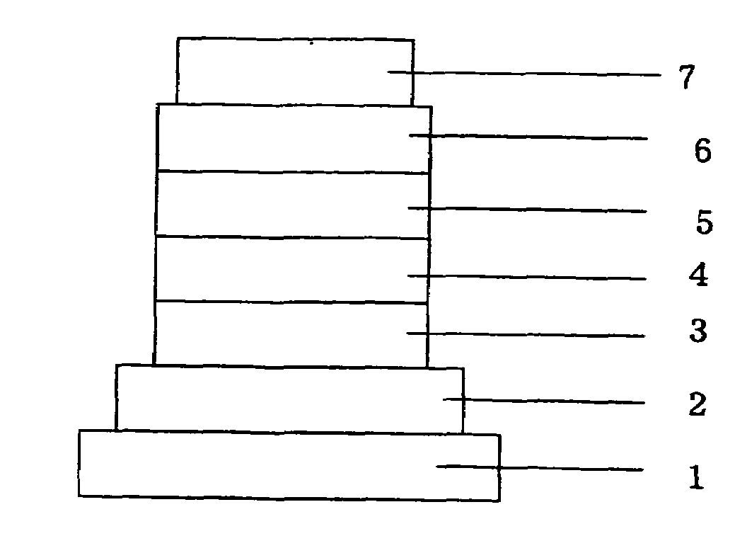
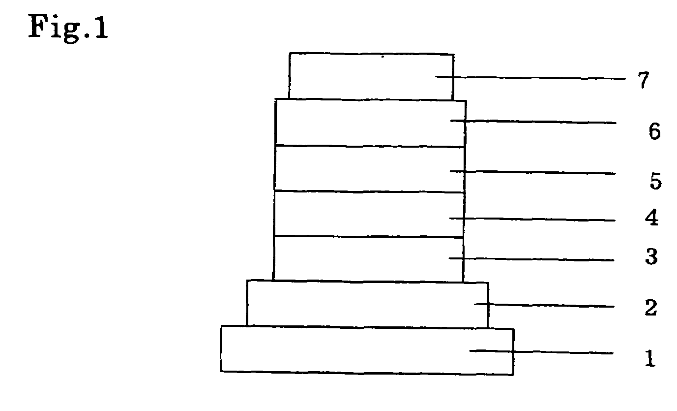
[0045]An organic EL device was constructed as in FIG. 1 with omission of a hole-injecting layer and addition of an electron-injecting layer. Constituent layers were piled one upon another in thin film on a glass substrate on which a 150 nm-thick ITO anode had been formed by the vacuum deposition process at a degree of vacuum of 4.0×10⁻⁴ Pa. First, NPB was deposited on the ITO anode to a thickness of 60 nm to form a hole-transporting layer.

[0046]Next, compound 1 and Ir(ppy)3 were codeposited from different evaporation sources on the hole-transporting layer to a thickness of 25 nm to form a light-emitting layer. The concentration of Ir(ppy)3 at this time was 7.0%. Then, Alq3 was deposited to a thickness of 50 nm to form an electron-transporting layer. Further, lithium fluoride (LiF) was deposited to a thickness of 0.5 nm to form an electron-injecting layer. Finally, aluminum (Al) as an electrode was deposited on the electron-injecting layer to a thickness of 170 nm to complete an orga...


PUM


Abstract

Disclosed is an organic electroluminescent device (organic EL device) which is improved in luminous efficiency, fully assured of driving stability, and simple in constitution. The organic electroluminescent device comprises a hole-transporting layer, a light-emitting layer, and an electron-transporting layer disposed between an anode and a cathode piled one upon another on a substrate and the light-emitting layer contains a phosphorescent dopant and an indolocarbazole compound of specific structure. Examples of the indolocarbazole compound are N,N′-diphenylindolocarbazole and bis(N-phenylindolo)carbazole.

Description

TECHNICAL FIELD[0001]This invention relates to an organic electroluminescent device (hereinafter referred to as organic EL device) and, more particularly, to an organic EL device that emits light of high luminance by simultaneous use of a phosphorescent dopant and a host compound of specific structure.BACKGROUND TECHNOLOGY[0002]An organic EL device of the simplest structure is generally constituted of a light-emitting layer sandwiched between a pair of counter electrodes and utilizes the following light-emitting phenomenon. Upon application of voltage to the electrodes, electrons are injected from a cathode and holes are injected from an anode and they recombine in the light-emitting layer; after recombination, the energy level in the conduction band goes back to the energy level in the valence band with release of energy in the form of light.[0003]In recent years, organic thin films have been used in the development of EL devices. In particular, devices that comprise a hole-transpo...

Claims


Application Information

Patent Timeline
IPC IPC(8): H01J1/63
CPCC09K11/06C09K2211/1029C09K2211/1037C09K2211/1074C09K2211/185H05B33/14H01L51/0078H01L51/0085H01L51/0087H01L51/5016H01L51/0072H10K85/311H10K85/6572H10K85/346H10K85/342H10K50/11H10K2101/10H10K50/12
Inventor ASARI, TOHRUYAMAMOTO, TOSHIHIROKOMORI, MASAKIKAI, TAKAHIRO
Owner NIPPON STEEL CHEMICAL CO LTD
Why Eureka
Try Eureka