High Speed Sense Amplifier Array and Method for Nonvolatile Memory

a high-speed sense amplifier and amplifier array technology, applied in static storage, digital storage, instruments, etc., can solve the problems of unsuitable mobile and handheld environment, bulky disk drives, and easy mechanical failure, and achieve the effect of reducing noise in the intermediate circui

Active Publication Date: 2009-12-03
SANDISK TECH LLC
View PDF28 Cites 42 Cited by
  • Summary
  • Abstract
  • Description
  • Claims
  • Application Information

AI Technical Summary

Benefits of technology

[0019]According to one set of aspects, this allows a method of sensing conduction current of non-volatile memory cells, where the method includes providing a node accessible by one or more memory cells via an intermediate circuit; precharging the node to an initial voltage for a first sensing operation; discharging the node through a first of the memory cells via the intermediate circuit; measuring the conduction current though the first memory cell by the rate of said discharging of the node; latching the result of said measuring; and outputting the latched result to a data bus. In one set of aspects, subsequent to said latching but prior to completing said outputting, precharging the node for a second sensing operation. In another set of aspects, the latched result is output to a data bus by a path independent of the node and the intermediate circuit. In a further aspect, outputting the latched result to a data bus independently of intermediate circuit reduces noise in the intermediate circuit.

Problems solved by technology

Conventional mass storage, based on rotating magnetic medium such as hard drives and floppy disks, is unsuitable for the mobile and handheld environment.
This is because disk drives tend to be bulky, are prone to mechanical failure and have high latency and high power requirements.
These undesirable attributes make disk-based storage impractical in most mobile and portable applications.
Additionally, the massively parallel memory page presents significant issues of noise and interference among the closely packed memory cells and structures that limit sensing accuracy and ultimately performance and storage capacity.

Method used


Image

  • High Speed Sense Amplifier Array and Method for Nonvolatile Memory
  • High Speed Sense Amplifier Array and Method for Nonvolatile Memory
  • High Speed Sense Amplifier Array and Method for Nonvolatile Memory

Examples


Embodiment Construction

Memory System

[0046]FIG. 1 to FIG. 11 illustrate example memory systems in which the various aspects of the present invention may be implemented.

[0047]FIG. 12 to FIG. 13 illustrate noise problems in existing sensing circuits.

[0048]FIG. 16 to FIG. 19 illustrate the various aspects and embodiments in which noise problems are addressed.

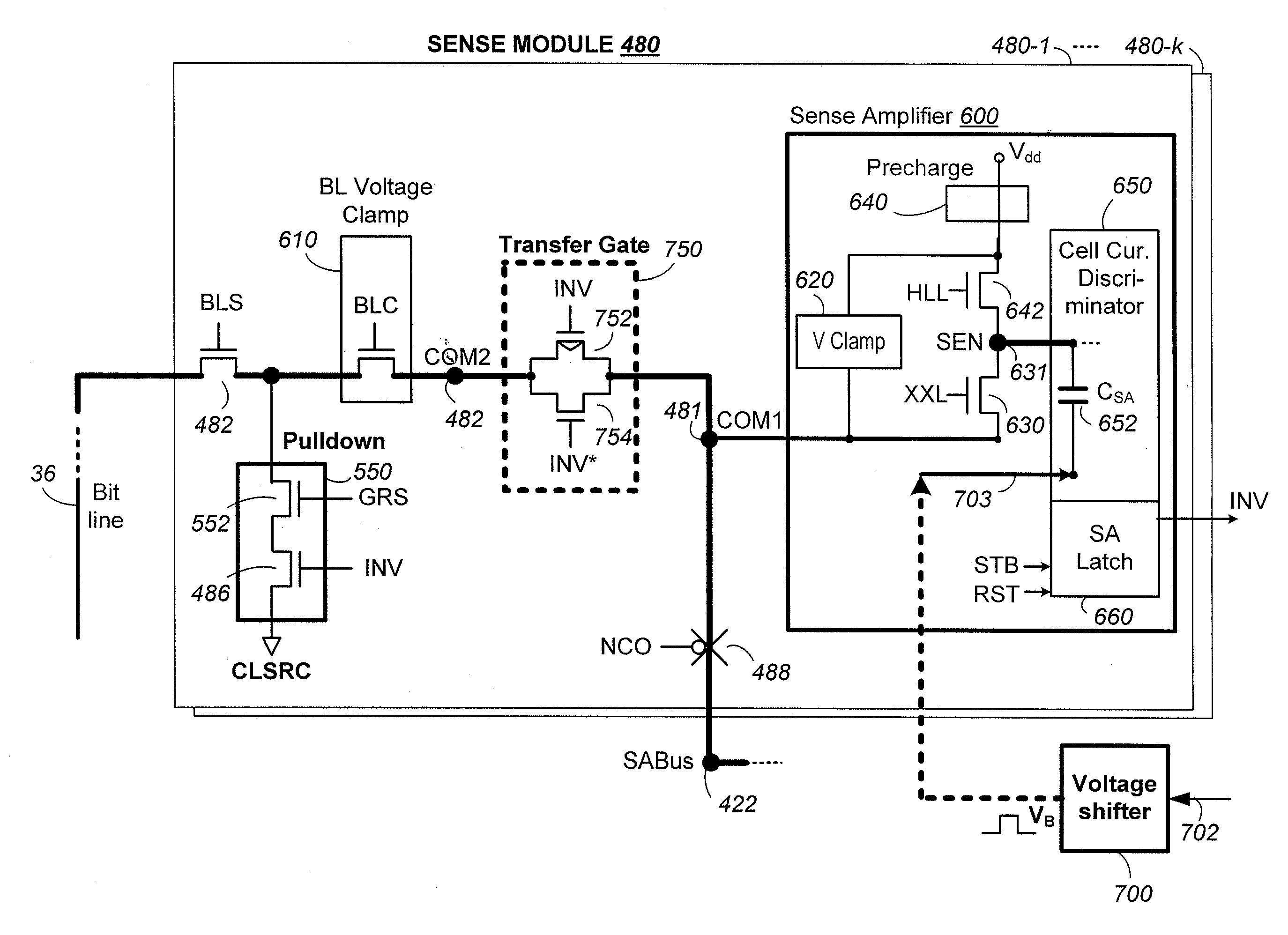
[0049]FIGS. 20A-C illustrate a sense module having a path for data transferal that overlaps the analog path for sensing.

[0050]FIGS. 21A-C illustrate a sense module having a path for data transferal that is distinct from the analog path for sensing.

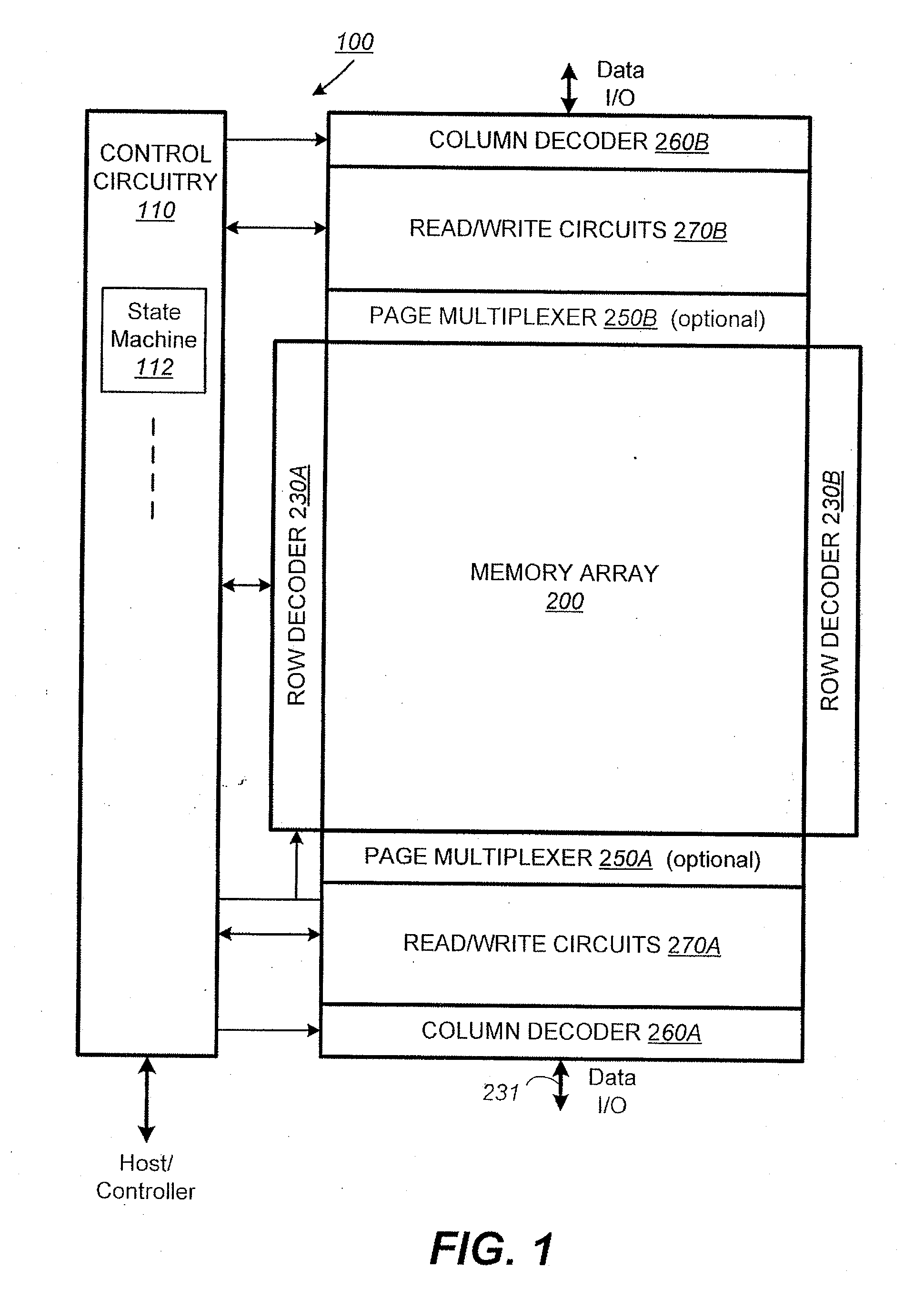
[0051]FIG. 1 illustrates schematically the functional blocks of a non-volatile memory chip in which the present invention may be implemented. The memory chip 100 includes a two-dimensional array of memory cells 200, control circuitry 210, and peripheral circuits such as decoders, read / write circuits and multiplexers.

[0052]The memory array 200 is addressable by word lines via row decoders 230 (split into 230A, 23...


PUM


Abstract

Sensing circuits for sensing a conduction current of a memory cell among a group of non-volatile memory cells being sensed in parallel and providing the result thereof to a data bus are presented. A precharge circuit is coupled to a node for charging the node to an initial voltage. An intermediate circuit is also coupled to the node and connectable to the memory cell, whereby current from the precharge circuit can be supplied to the memory cell. The circuit also includes a comparator circuit to perform a determination the conduction current by a rate of discharge at the node; a data latch coupled to the comparator circuit to hold the result of said determination; and a transfer gate coupled to the data latch to supply a result latched therein to the data bus independently of the node. This arrangement improves sensing performance and can help to eliminate noise on the analog sensing path during sensing and reduce switching current.

Description

FIELD OF THE INVENTION[0001]This invention relates generally to non-volatile semiconductor memory such as electrically erasable programmable read-only memory (EEPROM) and flash EEPROM, and specifically to sensing circuits and memory operations in speed is increased for the operation of sensing circuits.BACKGROUND OF THE INVENTION[0002]Solid-state memory capable of nonvolatile storage of charge, particularly in the form of EEPROM and flash EEPROM packaged as a small form factor card, has become the storage of choice in a variety of mobile and handheld devices, notably information appliances and consumer electronics products. Unlike RAM (random access memory) that is also solid-state memory, flash memory is non-volatile and retains its stored data even after power is turned off. In spite of the higher cost, flash memory is increasingly being used in mass storage applications. Conventional mass storage, based on rotating magnetic medium such as hard drives and floppy disks, is unsuitab...

Claims


Application Information

Patent Timeline
Patent Type & Authority Applications(United States)
IPC IPC(8): G11C16/26G11C7/00
CPCG11C7/02G11C7/06G11C2211/5634G11C16/0483G11C16/26G11C11/5642G11C5/063
Inventor NGUYEN, HAO THAIMUI, MAN LUNGLEE, SEUNGPILZHANG, FANGLINWANG, CHI-MING
Owner SANDISK TECH LLC
Why Eureka
Try Eureka