Photoelectric Converter and Method for Producing the Same
- Summary
- Abstract
- Description
- Claims
- Application Information
AI Technical Summary
Benefits of technology
Problems solved by technology
Method used
Image
Examples
embodiment 1
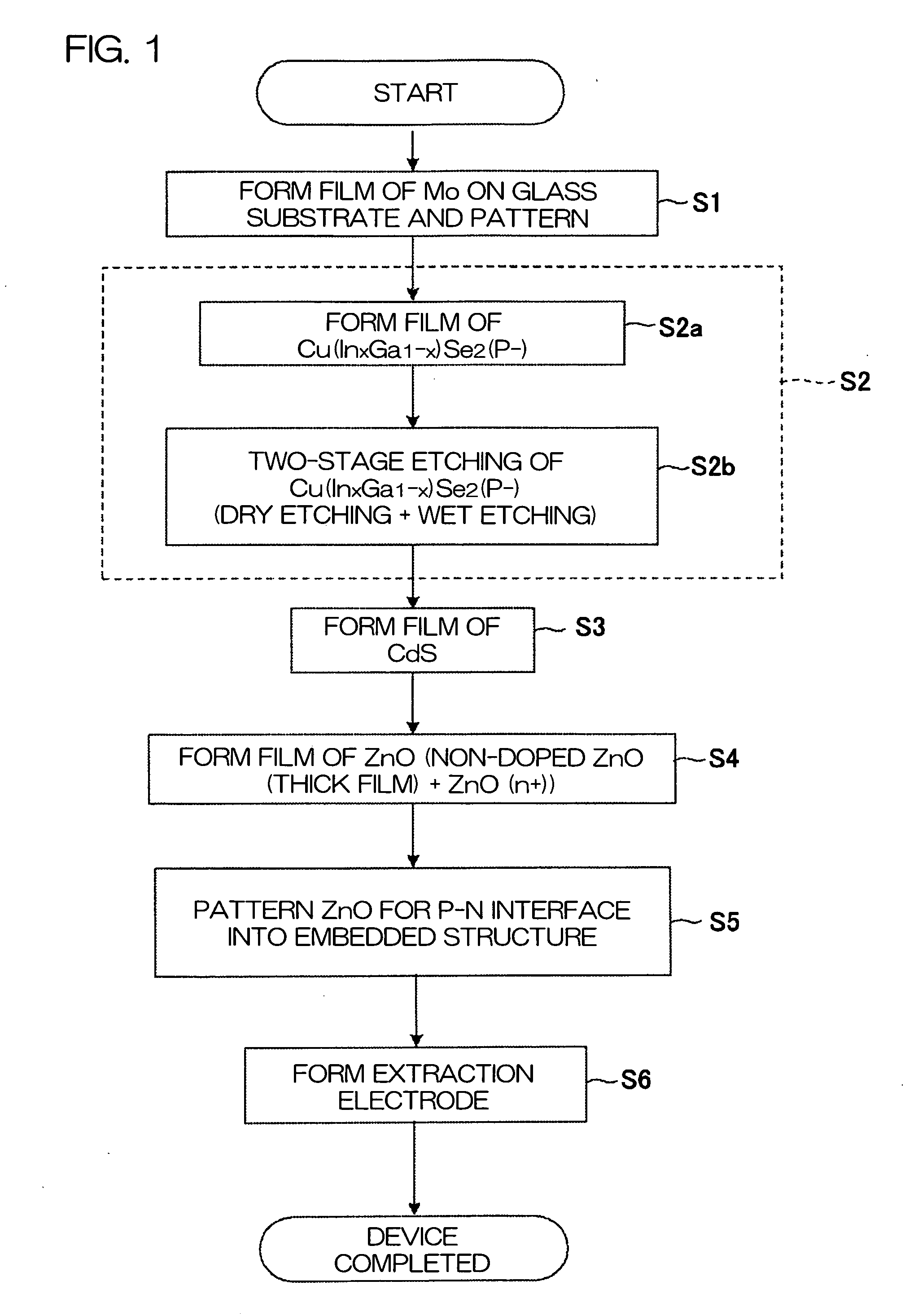
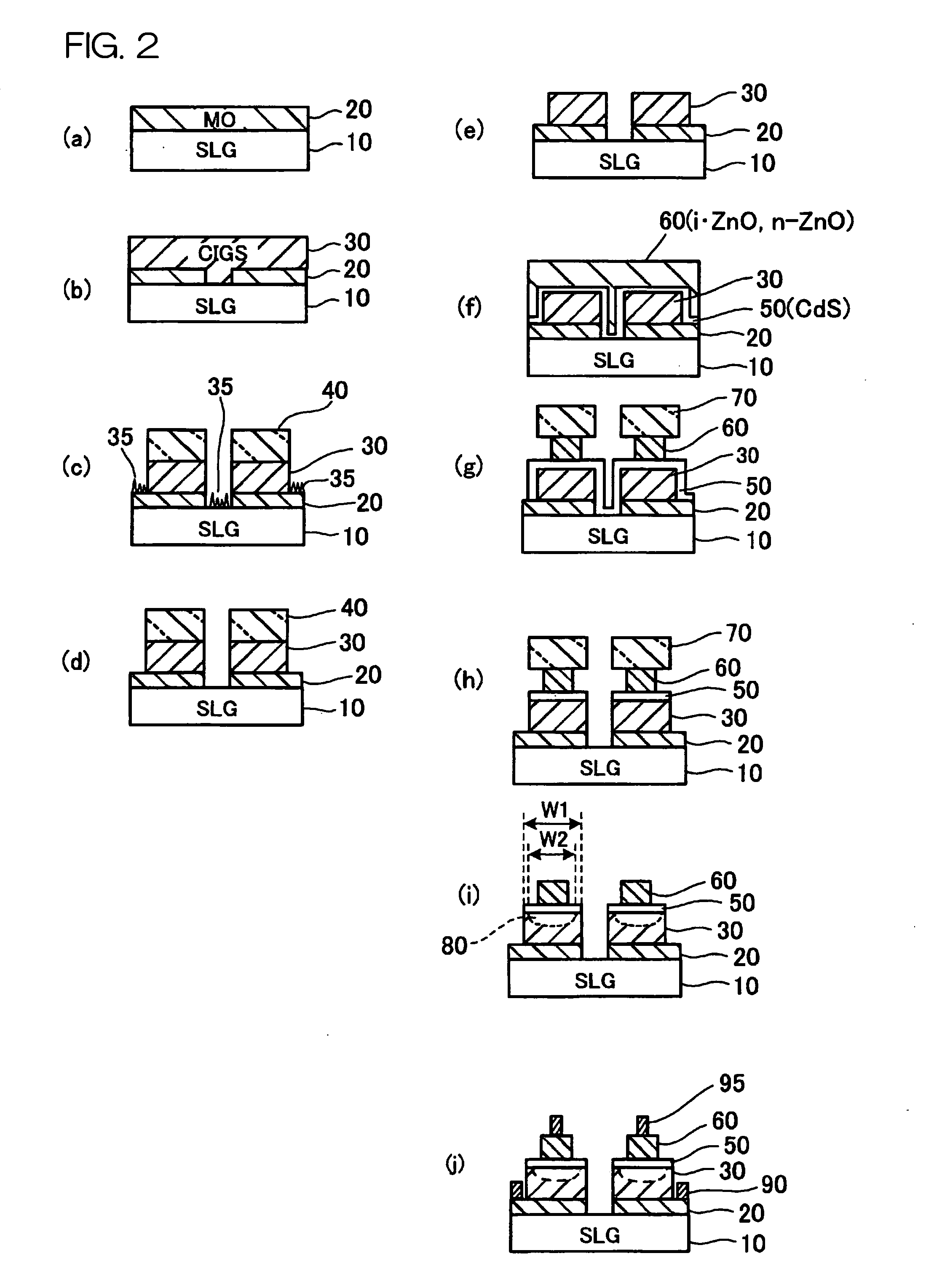
[0067]FIG. 1 is a flow chart showing an outline of principal steps of a method for producing a photoelectric converter according to the present invention. FIGS. 2(a) to 2(j) are step sectional views.
[0068]As shown in FIG. 2(j), the photoelectric converter according to the present invention is configured by sequentially laminating a lower electrode layer 20 made of a Mo thin film, a p-type semiconductor thin film (Cu(Inx,Ga(1-x))Se2 (0≦x≦1)) 30 with a chalcopyrite structure functioning as a photoabsorption (photoelectric conversion) layer and a light transmitting electrode layer on a substrate 10, the pattern of the light transmitting electrode layer is formed that an end of the compound semiconductor thin film with the chalcopyrite structure is positioned outward beyond an end of the light transmitting electrode layer, and the light transmitting electrode layer is made of a non-doped ZnO film 50 provided on the interface between the same and the compound semiconductor thin film and ...
embodiment 2
[0106]In this embodiment, an example of using the photoelectric converter according to the present invention as a photosensor having a high sensitivity also in the near infrared region is described.
[0107]FIG. 5 is a diagram showing absorption coefficients of a CIS thin film (also applies to a CIGS thin film) with respect to the wavelengths of light. As is illustrated, it is understood that the CIS film (CIGS thin film) has a high sensitivity over a wide range from visible light to near infrared light.
[0108]With attention drawn to this point, a composite image sensor is formed by laminating the photoelectric converter of the present invention made of a compound semiconductor thin film on a silicon substrate formed with a CMOS circuit in this embodiment.
[0109]FIG. 6 is a schematic sectional view of a general CMOS image sensor formed on a silicon substrate. FIG. 7 is a schematic sectional view of the composite image sensor according to the present invention formed by laminating the pho...
PUM
 Abstract
Description
Claims
Application Information


