Apparatus And Method For Image Sensor With Carbon Nanotube Based Transparent Conductive Coating

an image sensor and carbon nanotube technology, applied in the field of apparatus and method of image sensor with carbon nanotube transparent conductive coating, can solve the problems of difficult to achieve a high fill factor, inability to detect visible light in the sensor, and inability to achieve high fill factor

Active Publication Date: 2009-12-10
OMNIVISION TECH INC
View PDF10 Cites 26 Cited by
  • Summary
  • Abstract
  • Description
  • Claims
  • Application Information

AI Technical Summary

Benefits of technology

[0009]A backside illuminated image sensor includes a carbon nanotube transparent conductive coating formed on the backside of the image sensor using a low temperature process. The image sensor is designed to detect visible light. The carbon nanotube transparent conductive coating has characteristics selected so that the coating is at least semi-transparent to each wavelength of visible light that the image sensor is designed to d

Problems solved by technology

As a result, certain wavelengths of infrared light have the potential to degrade sensor detection of visible light.
However, a disadvantage of a FSI image sensor is that it is difficult to achieve a high fill factor, where the fill factor is the percentage of the pixel area sensitive to light.
However, a BSI image sensor typically requires that the substrate be thinned to reduce optical absorption.
However, an ITO TCC also has several undesirable c

Method used


Image

  • Apparatus And Method For Image Sensor With Carbon Nanotube Based Transparent Conductive Coating
  • Apparatus And Method For Image Sensor With Carbon Nanotube Based Transparent Conductive Coating
  • Apparatus And Method For Image Sensor With Carbon Nanotube Based Transparent Conductive Coating

Examples


Embodiment Construction

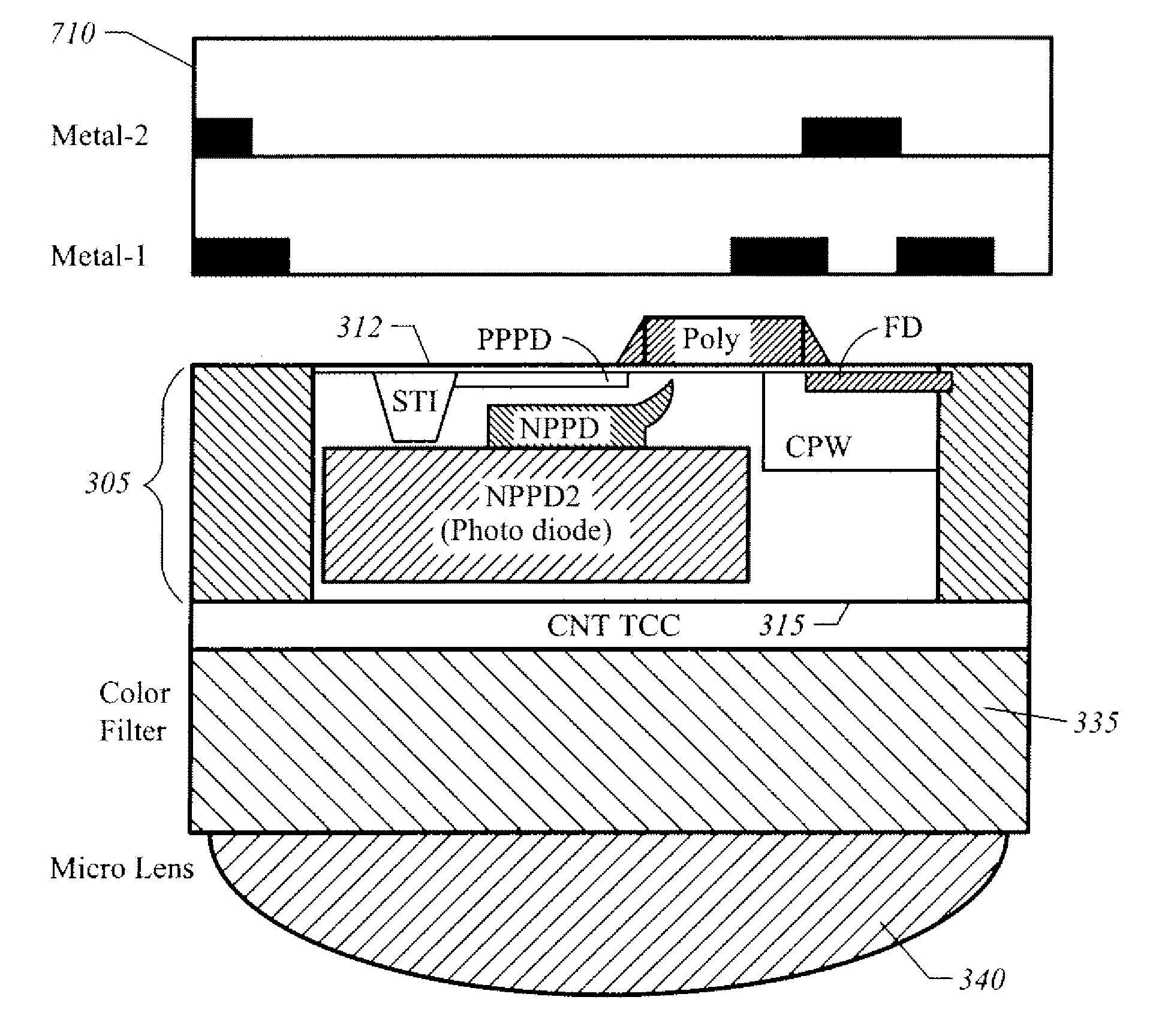
[0019]FIG. 3 illustrates a Back Side Illuminated (BSI) image sensor 300 in accordance with one embodiment of the present invention. In one embodiment BSI image sensor 300 is a CMOS image sensor formed on epitaxial silicon. A semiconductor substrate 305 has a front surface 310 and a back surface 315 (hereinafter “backside 315”). An array of photo-sensitive pixels 312 is formed in substrate 305. The substrate 305 is thinned such that a comparatively small thickness of epitaxial silicon 314 remains below pixels 312. For example, a conventional fabrication process may be used to perform front-side processing on a conventional silicon wafer, such as growing an epitaxial layer on a silicon wafer, performing masked diffusion processes to define n-doped and p-doped pixel regions of photodiodes and other pixel elements, and forming electrical contacts and electrical interconnections to the front-side. After front-side processing is completed the semiconductor wafer is thinned down (e.g., thi...


PUM


Abstract

A backside illuminated image sensor has a carbon nanotube transparent conductive coating formed on the backside of the image sensor. In one implementation the carbon nanotube transparent conductive coating acts as a wavelength selective filter to filter out infrared light. In one implementation the carbon nanotube transparent conductive coating has an optical transparency between 50% and 80% for blue and green color bands.

Description

FIELD OF THE INVENTION[0001]The present invention is generally related to techniques to provide a transparent conductive coating on the backside of a backside illuminated image sensor. More particularly, the present invention is directed to a backside illuminated image sensor having a carbon nanotube transparent conductive coating.BACKGROUND OF THE INVENTION[0002]Image sensors are typically formed on a semiconductor substrate. For example, Complementary Metal Oxide Semiconductor (CMOS) image sensors are typically formed on a silicon substrate. CMOS processes to fabricate photo-sensitive pixels comprising photodiodes are well known in the art and described in various patents by OmniVision Technologies, such as U.S. Pat. No. 7,355,228 and U.S. Pat. Pub. 20070072325, the contents of which are hereby incorporated by reference.[0003]In a Front-side Illuminated (FSI) arrangement the front-side of the image sensor receives the input light after the light passes through other front-side por...

Claims


Application Information

Patent Timeline
IPC IPC(8): H01L27/00B05D5/00
CPCB82Y10/00B82Y20/00H01L27/14609H01L27/1464H01L27/14685H01L31/02162H01L27/14621
Inventor MASSETTI, DOMINIC
Owner OMNIVISION TECH INC
Why Eureka
Try Eureka