
Intralevel conductive light shield

a conductive light shield and conductive technology, applied in the field of semiconductor structures, can solve the problems of large image degradation of image sensor pixels, small amount of charge leakage from floating drain nodes to the substrate, and noise due to leakage becomes a serious challenge, and achieve the effect of less prone to nois

Active Publication Date: 2009-12-10
GLOBALFOUNDRIES US INC
View PDF6 Cites 32 Cited by
  • Summary
  • Abstract
  • Description
  • Claims
  • Application Information

AI Technical Summary

Benefits of technology

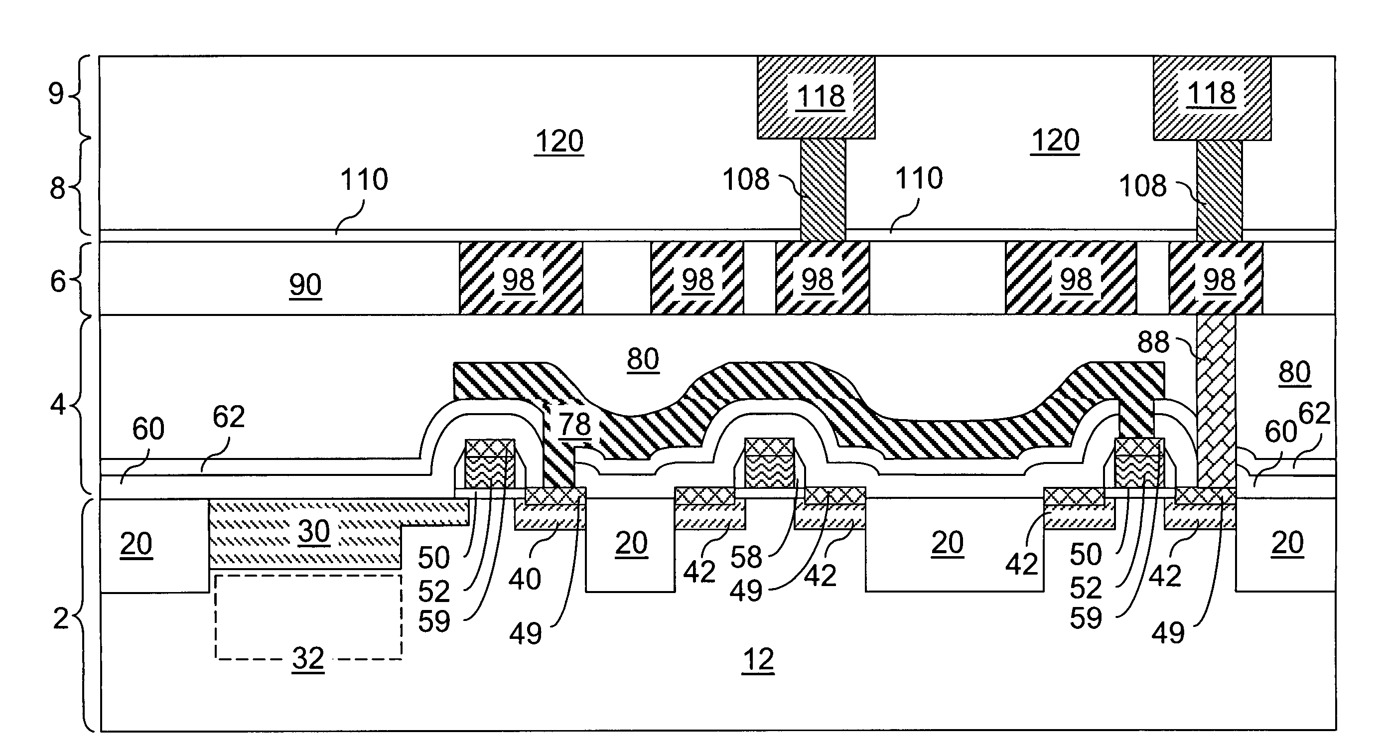
[0022]In the present invention, a conductive light shield is formed over a first dielectric layer of a via level in a metal interconnect structure. The conductive light shield covers a floating drain of an image sensor pixel cell. A second dielectric layer is formed over the conductive light shield and at least one via extending from a top surface of the second dielectric layer to a bottom surface of the first dielectric layer is formed in the metal interconnect structure. The conductive light shield may be formed within a contact level between a top surface of a semiconductor substrate and a first metal line level, or may be formed in any metal interconnect via level between two metal line levels. The inventive image sensor pixel cell is less prone to noise due to the blockage of light over the floating drain by the conductive light shield.

Problems solved by technology

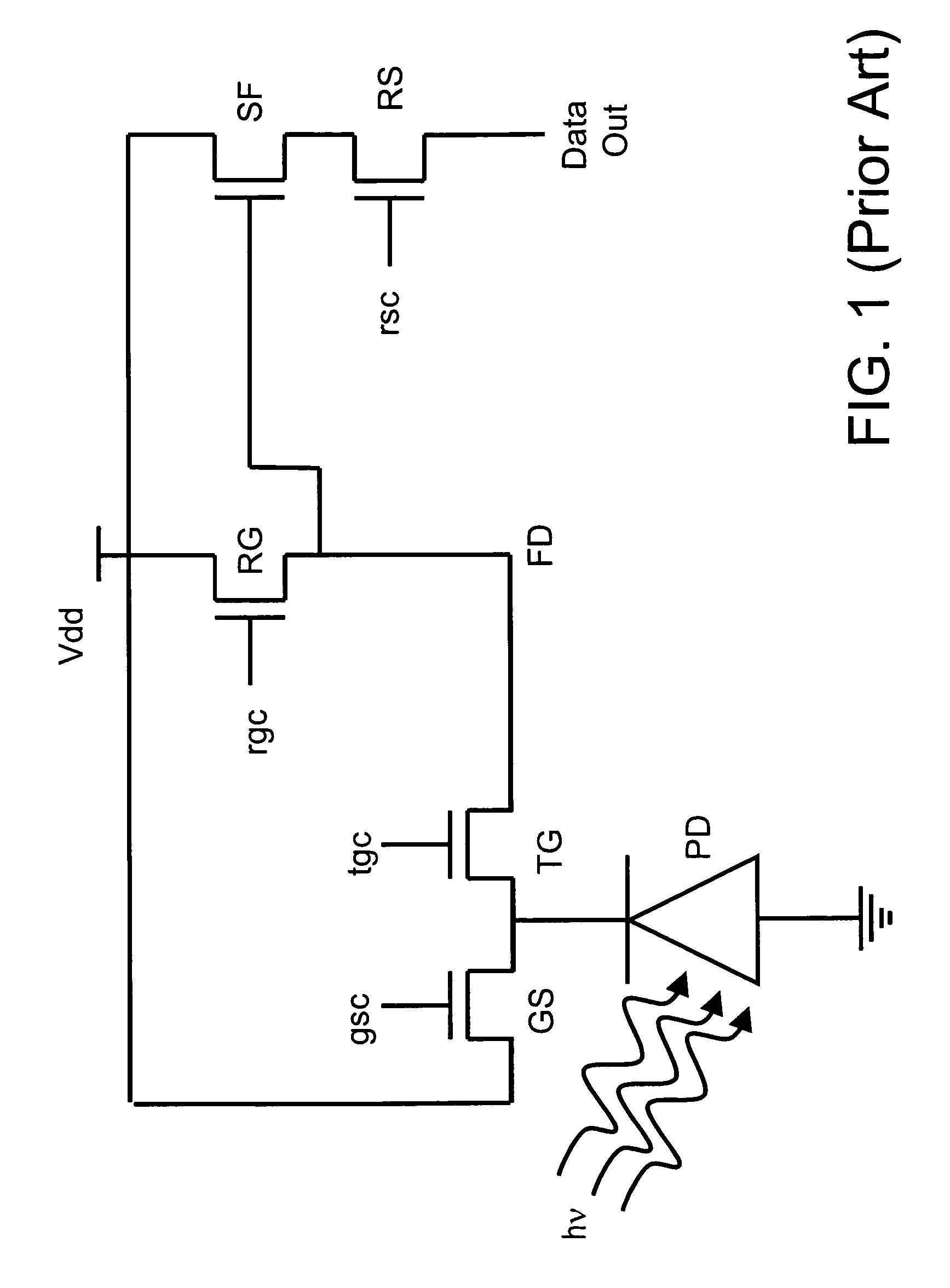
However, there is a small amount of leakage of charge from the floating drain node FD to the substrate, through the transfer gate transistor TG, and the reset gate transistor RG since leakage current paths are present in almost every device.
In practical terms, the most significant leakage is typically the leakage through the reset gate transistor.
The greater the leakage, the greater the shift in the voltage during the hold time, and consequently, the greater the degree of image degradation from the array of the image sensor pixels.
Thus, the noise due to leakage becomes a serious challenge in a global shutter method, which is employed in many CMOS image sensors to enable capture of images of high speed objects.
The global shutter method enables image capture of high speed subjects without image artifacts, but introduces a concern with the global shutter efficiency of the pixel since the integrity of the signal may be compromised by any charge leakage from the floating diffusion between the time of the image capture and the time of the reading of the imager array.
In practice, this is not the case due to the charge leakage and / or charge generation, and the picture quality is correspondingly degraded.
The wiring of the metal interconnect level thus becomes restrictive to accommodate the light shield.
In some cases, adding a light shield with accompanying changes to interconnect wiring structures may require increasing the wiring channels, which can adversely degrade the effective fill factor of the image sensor pixel used for light collection, or may add unnecessary capacitance to the floating diffusion.

Method used


Image

  • Intralevel conductive light shield
  • Intralevel conductive light shield
  • Intralevel conductive light shield

Examples


first embodiment

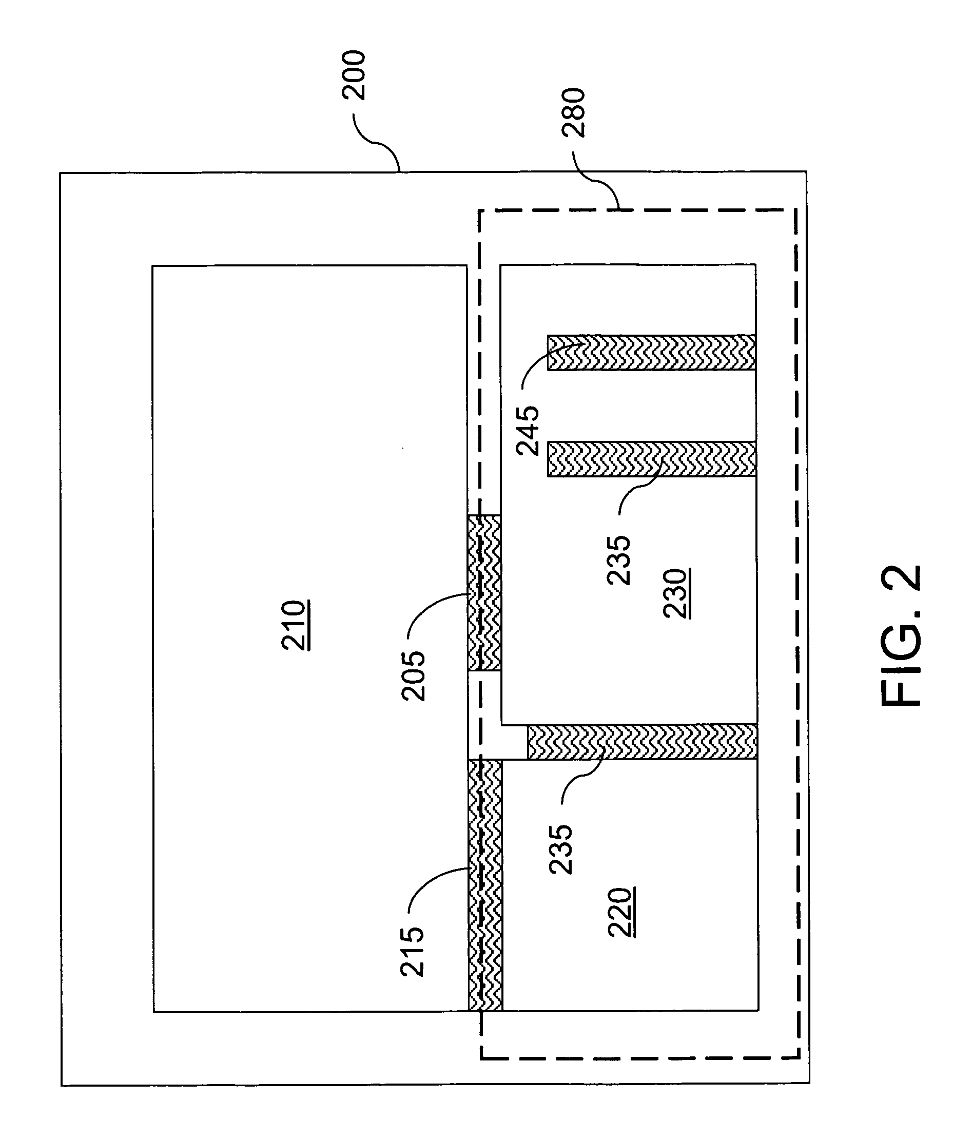
[0073]Referring to FIG. 3, a first exemplary semiconductor structure according to the present invention comprises a semiconductor substrate 2, a substrate contact via level interconnect structure 4, a first metal line level interconnect structure 6, a first back-end-of-line (BEOL) via level interconnect structure 8, and a second metal line level interconnect structure 9, which may be employed as a unit image sensor pixel 200 of FIG. 2.

[0074]The semiconductor substrate 2 comprises a semiconductor layer 12 having a doping of a first conductivity type, shallow trench isolation structures 20, a second conductivity type charge collection well 30, a floating drain 40, and source and drain regions 42 of field effect transistors, which may include a global reset transistor, a reset gate transistor, a source follower transistor, and a row select transistor. The semiconductor layer 12 includes a portion located directly underneath the second conductivity type charge collection well 30, which ...

fourth embodiment

[0134]Two dielectric layers encapsulate the conductive light shield 124 of the Specifically, the entirety of the surfaces of the conductive light shield 124 abut the lower second level dielectric layer 120A and the upper second level dielectric layer 120B, and the conductive light shield 124 is encapsulated by the second level dielectric layer (120A, 120B).

[0135]The back-end-of-line dielectric capping layer 110, the lower second level dielectric layer 120A, the lower portion of the upper second level dielectric layer 120B, the conductive light shield 124, the metal resistor 122, the first-type second level vias 108′, and the second-type second level vias 109 collectively constitute the first back-end-of-line (BEOL) via level interconnect structure 8. The upper portion of the upper second level dielectric layer 120B and the second metal lines 118 collectively constitute the second metal line level interconnect structure 9. Additional via level interconnect structures (not shown) and...

fifth embodiment

[0146]Two dielectric layers encapsulate the conductive light shield 124 of the Specifically, the entirety of the stack of the conductive light shield 124 and the dielectric portion 134 abut the lower second level dielectric layer 120A and the upper second level dielectric layer 120B, and stack of the conductive light shield 124 and the dielectric portion 134 is encapsulated by the second level dielectric layer (120A, 120B). Thus, the conductive light shield 124 is encapsulated by the second level dielectric layer (120A, 120B).

[0147]The lower capacitor electrode 122′, the node dielectric 132, and the upper capacitor electrode 142 collectively constitute a metal-insulator-metal capacitor (MIMCAP). The back-end-of-line dielectric capping layer 110, the lower second level dielectric layer 120A, the lower portion of the upper second level dielectric layer 120B, the conductive light shield 124, the dielectric portion 134, the MIMCAP (122′, 132, 142), the first-type second level vias 108′...


PUM


Abstract

A conductive light shield is formed over a first dielectric layer of a via level in a metal interconnect structure. The conductive light shield is covers a floating drain of an image sensor pixel cell. A second dielectric layer is formed over the conductive light shield and at least one via extending from a top surface of the second dielectric layer to a bottom surface of the first dielectric layer is formed in the metal interconnect structure. The conductive light shield may be formed within a contact level between a top surface of a semiconductor substrate and a first metal line level, or may be formed in any metal interconnect via level between two metal line levels. The inventive image sensor pixel cell is less prone to noise due to the blockage of light over the floating drain by the conductive light shield.

Description

RELATED APPLICATIONS[0001]The present application is related to co-pending U.S. application Ser. No. ______ (Attorney Docket No: BUR920080098US2); which is incorporated herein by reference.FIELD OF THE INVENTION[0002]The present invention relates to semiconductor structures, and more particularly to semiconductor structures incorporating a conductive light shield, and methods of manufacturing the same.BACKGROUND OF THE INVENTION[0003]A pixel sensor includes an array of pixel sensor cells that detects two dimensional signals. Pixel sensors include image sensors, which may convert a visual image to digital data that may be represented by a picture, i.e., an image frame. The pixel sensor cells are unit devices for the conversion of the two dimensional signals, which may be a visual image, into the digital data. A common type of pixel sensors includes image sensors employed in digital cameras and optical imaging devices. Such image sensors include charge-coupled devices (CCDs) or comple...

Claims


Application Information

Patent Timeline
IPC IPC(8): H01L21/768
CPCH01L23/552H01L27/14623H01L27/14636H01L2924/0002H01L2924/00
Inventor GAMBINO, JEFFREY P.HE, ZHONG-XIANGOGG, KEVIN N.RASSEL, RICHARD J.RASSEL, ROBERT M.
Owner GLOBALFOUNDRIES US INC
Learn More