Waveguide connection structure

a technology of connection structure and waveguide, which is applied in the direction of waveguides, waveguide type devices, basic electric elements, etc., can solve the problems of large transmission loss of electromagnetic waves at the connection area, and achieve the connection characteristics of waveguides, reduce leakage, and reduce signal loss

Active Publication Date: 2009-12-17
MITSUBISHI ELECTRIC CORP
View PDF3 Cites 15 Cited by
  • Summary
  • Abstract
  • Description
  • Claims
  • Application Information

AI Technical Summary

Benefits of technology

[0009]According to the present invention, it is configured such that the E-side edge of the waveguide is closed-ended by suppressing the parallel plate mode between the multilayer dielectric substrate and the metal substrate by a magnetic wall (open-ended in a standing wave) formed on an end of a conductor pattern in addition to the choke structure. Thus, it is possible to achieve the connection characteristics of the waveguides with lower leakage and lower loss of signals at the connection area of the waveguides, and to prevent the degradation of the connection characteristics that occurs in a conventional tec...

Problems solved by technology

As a result, there is a problem that a leaky wave in a parallel plate mode occurs between metal conductor...

Method used


Image

  • Waveguide connection structure
  • Waveguide connection structure
  • Waveguide connection structure

Examples


Embodiment Construction

[0031]Exemplary embodiments of the present invention are explained in detail below with reference to the accompanying drawings. The present invention is not limited to the embodiments.

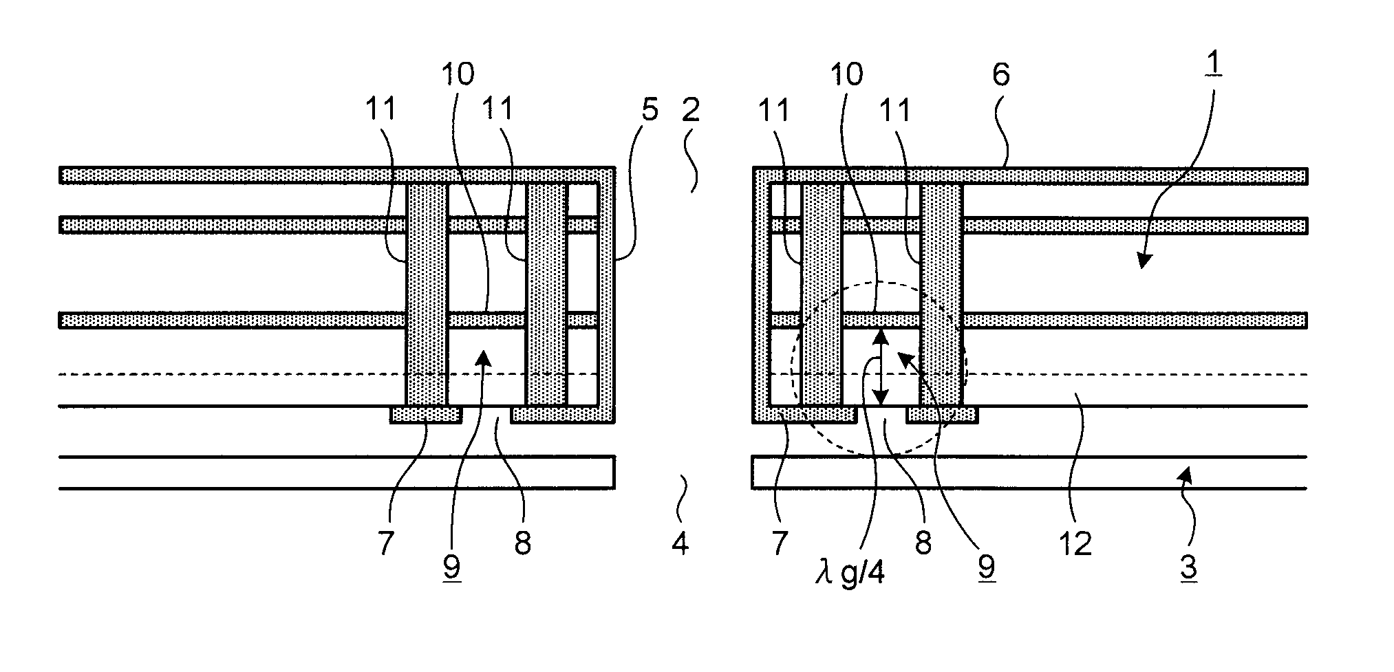
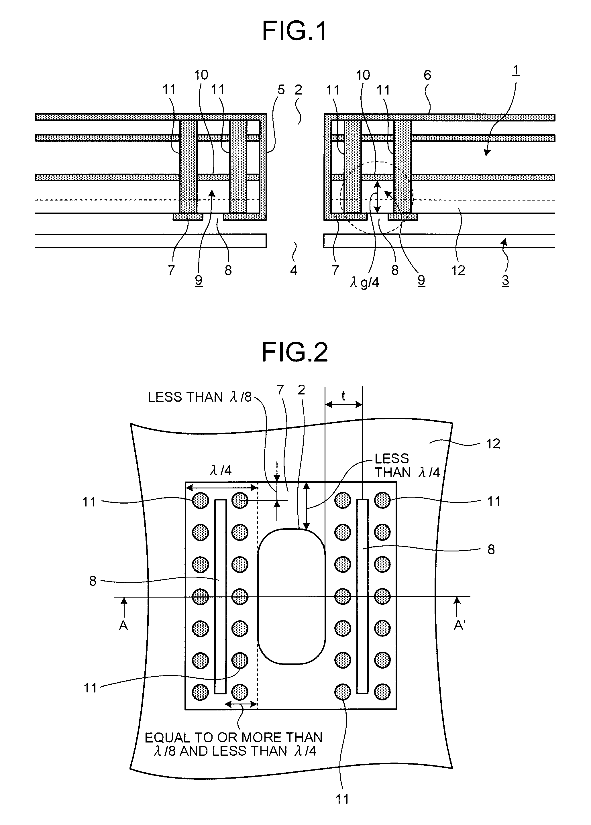
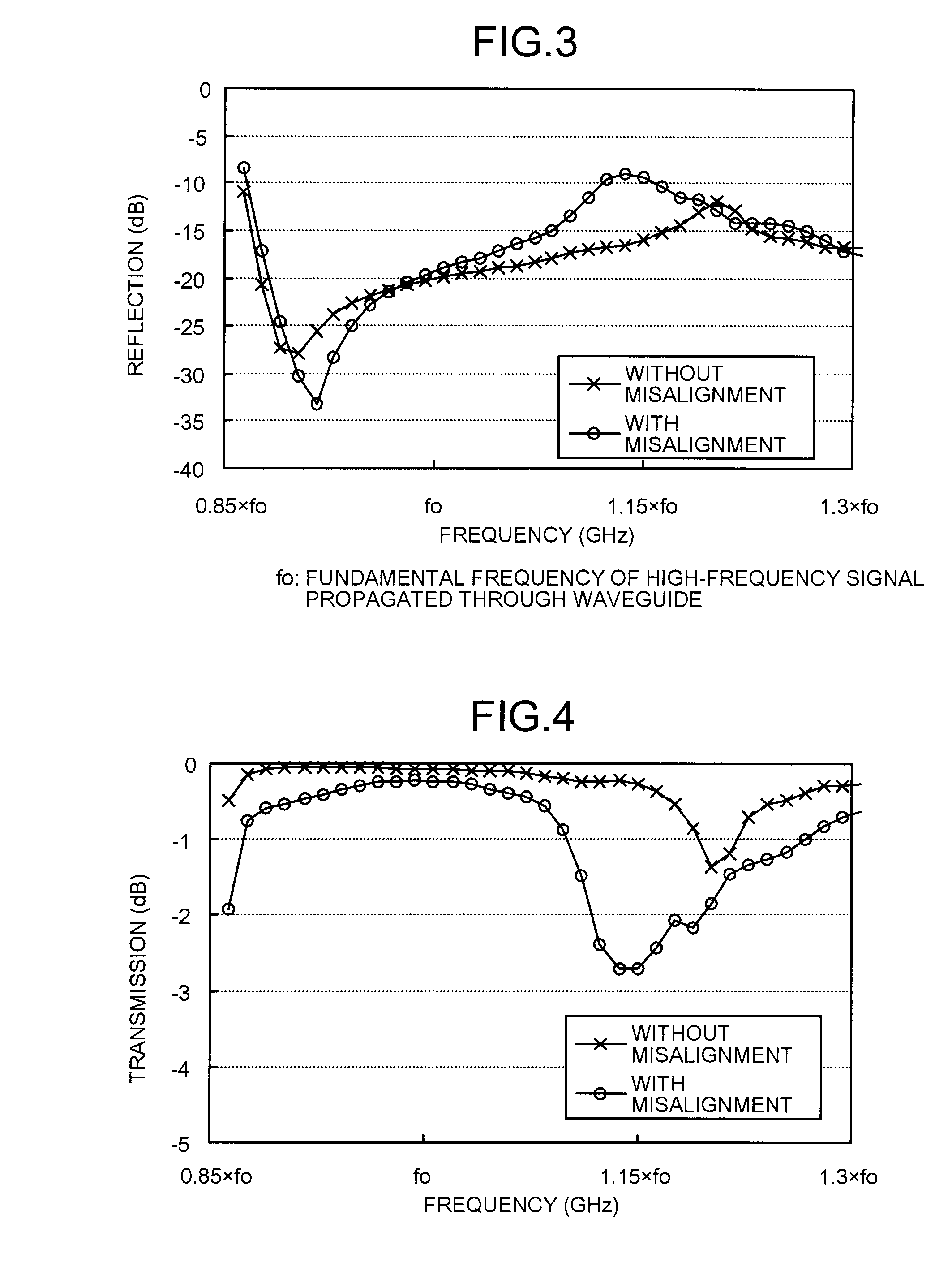
[0032]The embodiment of the present invention will be described below with reference to FIGS. 1 and 2. FIG. 1 is a cross section of a waveguide connection structure according to the embodiment. FIG. 2 is a plan view of a conductor pattern portion (land portion). The cross section shown in FIG. 1 corresponds to a cross section taken along a line A-A′ in FIG. 2. The waveguide connection structure according to the embodiment is applied to, for example, a millimeter-wave or microwave radar, such as an FM / CW radar.

[0033]A hollow waveguide 2 having a substantially rectangular shape at cross section is formed in a multilayer dielectric substrate 1 in its layer direction, and a hollow waveguide 4 having a substantially rectangular shape at cross section is formed in a metal substrate 3 such that the waveguide ...


PUM


Abstract

A rectangular conductor pattern is formed around a first waveguide on a multilayer dielectric substrate facing a metal substrate, with an end at about λ/4 away from a long side edge of the first waveguide, where λ is a free-space wavelength of a signal wave. A conductor opening is formed between the end of the conduction pattern and the long side edge of the first waveguide, with a length longer than a long side of the first waveguide and shorter than about λ. A closed-ended dielectric transmission path is formed in the multilayer dielectric substrate in the layer direction, with a length of about λg/4, where λg is an in-substrate effective wavelength of the signal wave.

Description

TECHNICAL FIELD[0001]The present invention relates to a waveguide connection structure for connecting a hollow waveguide formed in a multilayer dielectric substrate in its layer direction and a waveguide formed in a metal substrate.BACKGROUND ART[0002]In a conventional waveguide connection structure by which a waveguide (through hole) arranged in an organic dielectric substrate (connecting member) to transmit an electromagnetic wave is connected to a waveguide arranged in a metal waveguide substrate, a conductor on the through hole and the metal waveguide substrate are electrically connected to each other and are maintained at the same electric potential, so that reflection, transmission loss, and leakage of the electromagnetic wave are prevented at a connection area of the waveguides (for example, see Patent document 1).[0003]In the conventional waveguide connection structure disclosed in Patent document 1, a gap is formed between a conductor layer on the through hole and the waveg...

Claims


Application Information

Patent Timeline
IPC IPC(8): H01P1/04
CPCH01P3/121H01P1/042
Inventor SUZUKI, TAKUYA
Owner MITSUBISHI ELECTRIC CORP
Why Eureka
Try Eureka