Ferroelectric memory device, method for driving ferroelectric memory device, and electronic equipment

a ferroelectric memory device and readout technology, applied in the direction of information storage, static storage, digital storage, etc., can solve the problem of insufficient potential of ferroelectric capacitors, and achieve the effect of improving the readout margin

Inactive Publication Date: 2009-12-17
FUJITSU SEMICON LTD
View PDF4 Cites 17 Cited by
  • Summary
  • Abstract
  • Description
  • Claims
  • Application Information

AI Technical Summary

Benefits of technology

[0029]According to the method described above, the first node is set to a negative potential by the first capacitor before readout, and the potential on the first node can be converted to a positive potential by the first capacitor at the time of readout. Therefore, there is no need to provide a

Problems solved by technology

As a result, an adequate potential is not applied to ferro

Method used


Image

  • Ferroelectric memory device, method for driving ferroelectric memory device, and electronic equipment
  • Ferroelectric memory device, method for driving ferroelectric memory device, and electronic equipment
  • Ferroelectric memory device, method for driving ferroelectric memory device, and electronic equipment

Examples


embodiment 1

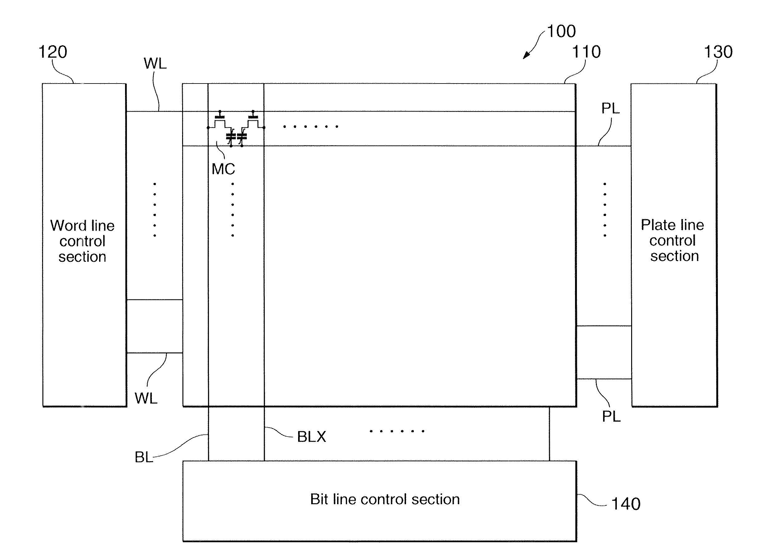
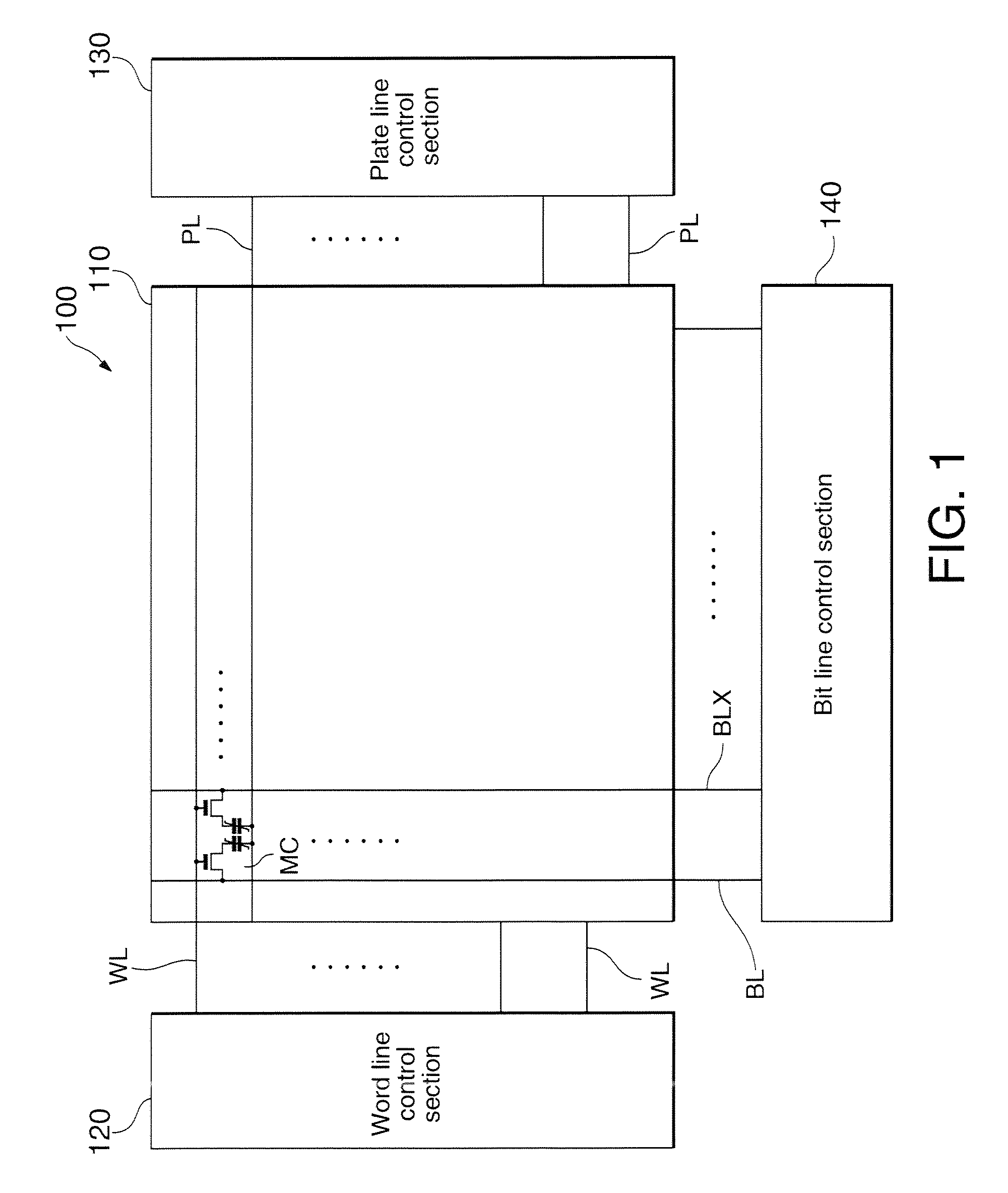
[0043]FIG. 1 is a block diagram of the structure of a ferroelectric memory device. As shown in the figure, a ferroelectric memory device 100 includes a memory cell array 110 and peripheral circuit sections (for example, 120, 130, 140, etc.). The memory cell array 110 is formed from a plurality of memory cells MC arranged in an array, wherein each of the memory cells MC is disposed at an intersection between a word line WL and a bit line (BL, BLX). In this embodiment, a 2T2C cell is shown as an example. In this case, each data set is stored by two transistors and two ferroelectric capacitors connected to a bit line BL and a bit line BLX, respectively. Also, the peripheral circuit may include a word line control section 120 and a plate line control section 130 which control voltages on a plurality of word lines WL and a plurality of plate lines PL. By the aforementioned control sections, data stored in the memory cells MC are readout onto the plurality of bit lines BL, or externally s...

embodiment 2

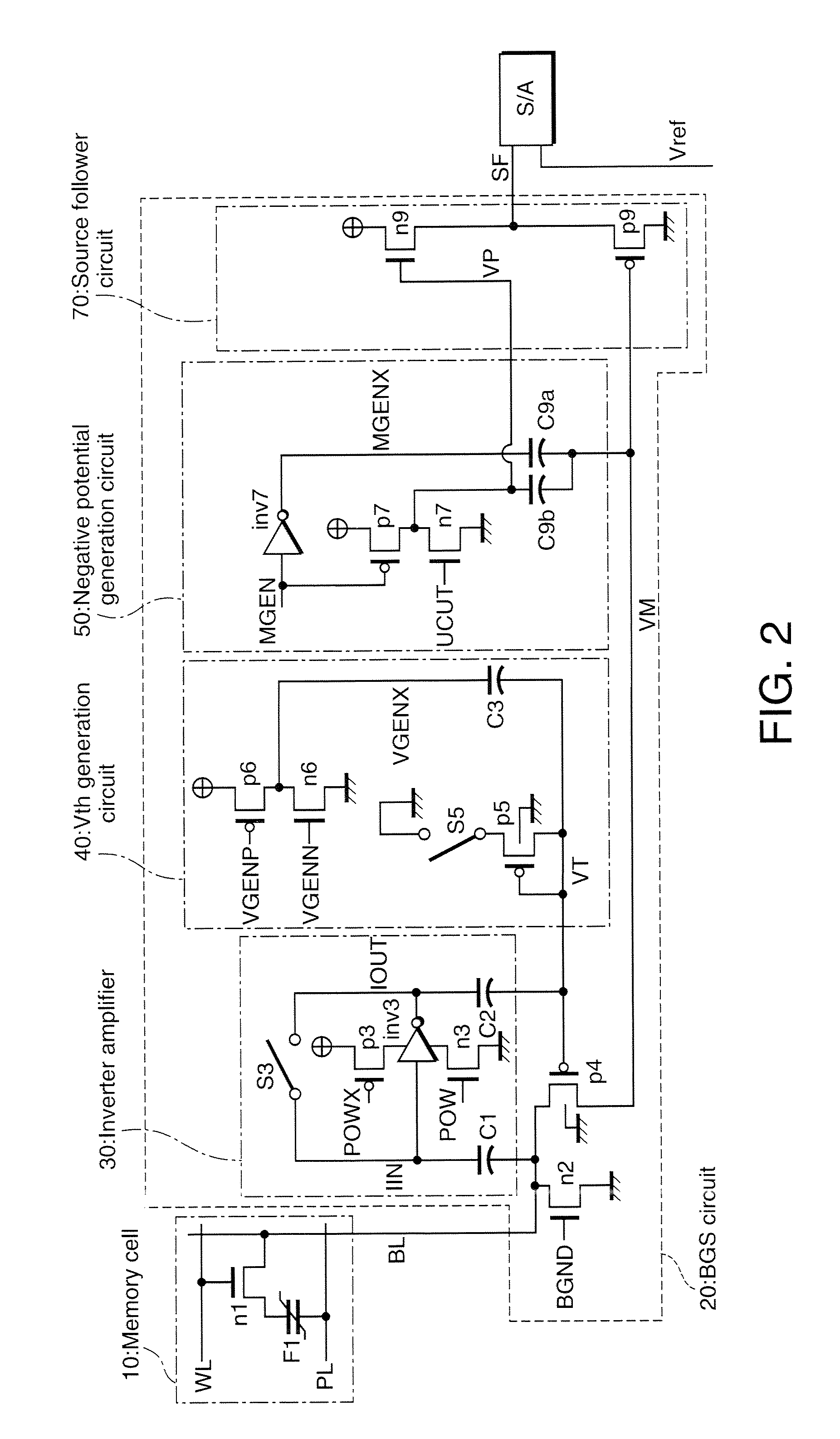
[0083]The embodiment 1 uses the source follower circuit 70, but the source follower circuit may be omitted.

[0084]FIG. 9 is a circuit diagram showing the structure of a readout circuit of the ferroelectric memory device in accordance with the present embodiment. It is noted that components in FIG. 9 identical with those of the embodiment 1 (shown in FIG. 2) shall be appended with the same reference numerals, and their detailed description shall be omitted.

[0085]As shown in FIG. 9, in accordance with the embodiment 2, a source follower circuit 70 is omitted, and the node VP is directly connected to a first input terminal of the sense amplifier S / A. In accordance with the present embodiment, the memory cell has a 2T2C cell structure; and among a bit line pair (BL and BLX), the bit line BLX is also connected to a similar BGS circuit 20. Accordingly, a node VPX, corresponding to the node VP, is connected to a second input terminal of the sense amplifier S / A, and these potentials are comp...


PUM


Abstract

A ferroelectric memory device includes: a memory cell having a ferroelectric capacitor connected between a plate line and a bit line; a first node connected to the bit line through a charge transfer MISFET; a potential generation circuit that has a first capacitor having a first terminal connected to the first node and a first switching MISFET connected to a second terminal of the first capacitor, and is capable of setting the first node to a negative potential; and a sense amplifier connected to the second terminal of the first capacitor. When reading a charge stored in the ferroelectric capacitor, the potential generation circuit sets the first node at a negative potential and then sets the first switching MISFET to an off state, thereby setting the second terminal of the first capacitor to a floating state, and the sense amplifier amplifies a potential on the second terminal of the first capacitor in the floating state.

Description

[0001]The entire disclosure of Japanese Patent Application No. 2008-155679, filed Jun. 13, 2008 is expressly incorporated by reference herein.BACKGROUND[0002]1. Technical Field[0003]The present invention relates to ferroelectric memory devices, and in particular, to readout technology for ferroelectric memory devices.[0004]2. Related Art[0005]For reading a ferroelectric memory device (FeRAM: Ferroelectric Random Access Memory), a method employing a latch-type sense amplifier circuit may be used. In this case, the voltage applied to the plate line is voltage-divided between the ferroelectric capacitor capacitance (Cs) and the bit line capacitance (Cbl). As a result, an adequate potential is not applied to ferroelectric capacitors due to the bit line capacitance (Cbl). Furthermore, because differences in bit line voltages are amplified by a sense amplifier and readout, the more the bit line capacitance (Cbl) increases, the smaller the bit line voltage becomes, so that the sense margin...

Claims


Application Information

Patent Timeline
IPC IPC(8): G11C11/22G11C11/24
CPCG11C11/22
Inventor KOIDE, YASUNORI
Owner FUJITSU SEMICON LTD
Why Eureka
Try Eureka