Avalanche Photodiode

a photodiode and avalanche technology, applied in the field of photodiodes, can solve the problems of serious sacrifice of alignment error, limited bandwidth of drift time, and prior art does not fulfill all users' requests on actual use, so as to achieve the effect of reducing bandwidth limitation and improving alignment error without sacrificing component velocity

Inactive Publication Date: 2009-12-24
NAT CENT UNIV
View PDF0 Cites 28 Cited by
  • Summary
  • Abstract
  • Description
  • Claims
  • Application Information

AI Technical Summary

Benefits of technology

[0004]The main purpose of the present invention is to relieve a bandwidth limit from a conflict between RC bandwidth and carrier transferring time and to en large an active area and improve alignment error without sacrificing component velocity.

Problems solved by technology

As shown in FIG. 7, hole from the multiplication layer has to pass through the thick absorption layer for drifting back to p-type electrode, which seriously limits bandwidth of drift time.
At the same time, alignment error is seriously sacrificed too.
Hence, the prior art does not fulfill all users' requests on actual use.

Method used


Image

  • Avalanche Photodiode
  • Avalanche Photodiode
  • Avalanche Photodiode

Examples


Embodiment Construction

[0017]The following description of the preferred embodiment is provided to understand the features and the structures of the present invention.

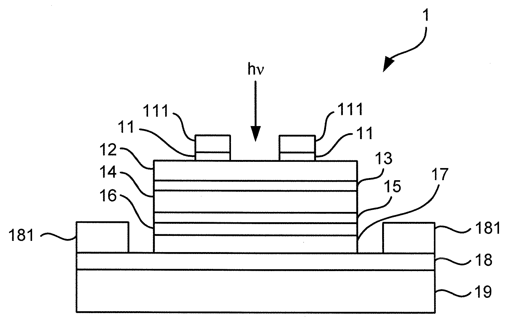
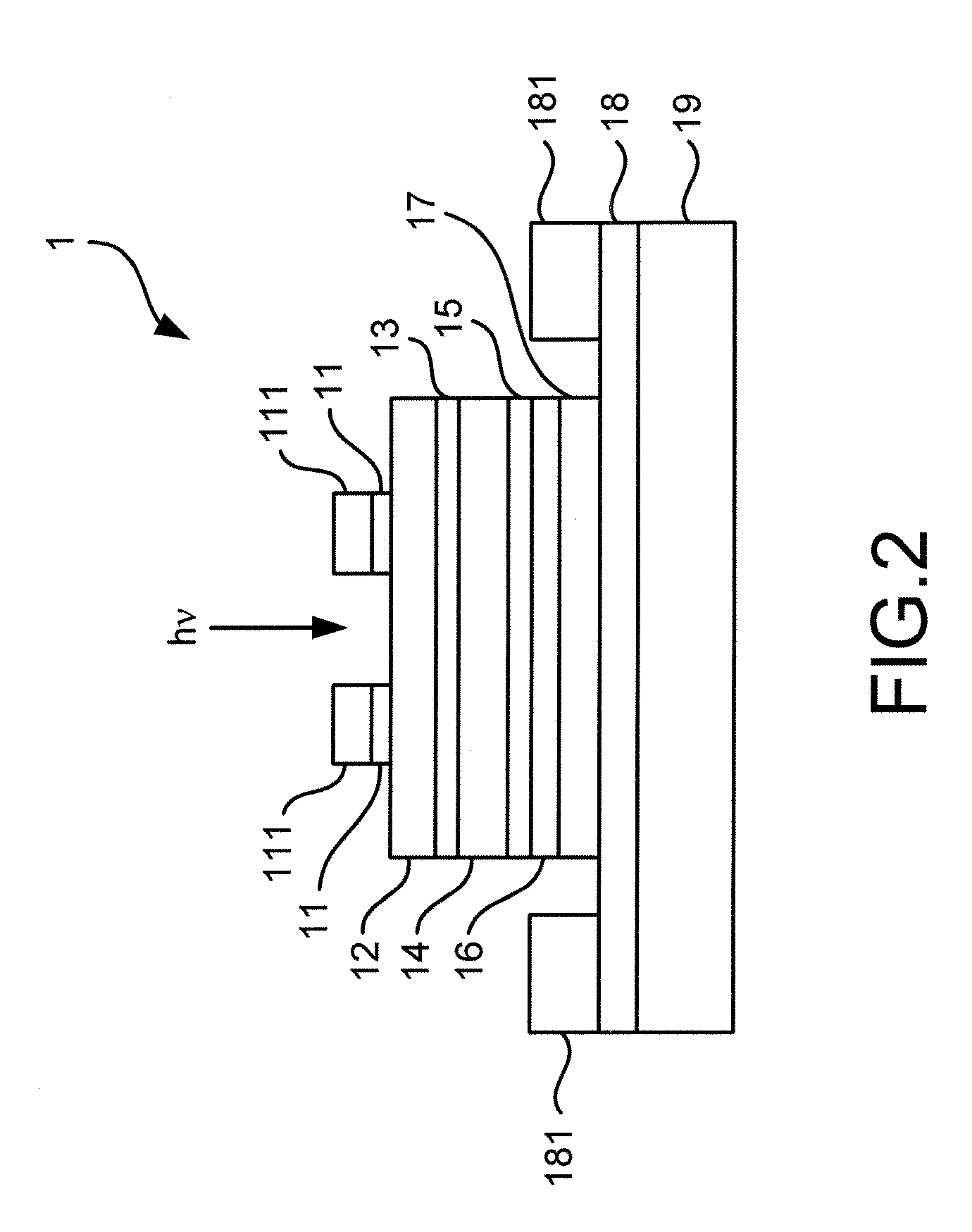
[0018]Please refer to FIG. 1 to FIG. 4B, which are a view showing energy band of a first preferred embodiment according to the present invention; sectional views showing a first and a second preferred embodiments; and views showing electron velocity and hole velocity. As shown in the figures, the present invention is an avalanche photodiode, from top to bottom comprising an epitaxial structure 1 of an n-type ohmic contact layer 11, a transport layer 12, a first graded bandgap layer 13, an absorption layer 14, a second graded bandgap layer 15, an n-type charge layer 16, a multiplication layer 17 and a p-type ohmic contact layer 18, where the epitaxial structure 1 thus obtains an n-i-n-i-p junction and is grown on a semi-insulating or conductive semiconductor substrate; and the present invention may further comprises an n-type metal conductive ...


PUM


Abstract

The present invention changes layer polarities of an epitaxy structure of an avalanche photodiode into n-i-n-i-p. A transport layer is deposed above an absorption layer to prevent absorbing photon and producing electrons and holes. A major part of electric field is concentrated on a multiplication layer for producing avalanche and a minor part of the electric field is left on the absorption layer for transferring carrier without avalanche. Thus, bandwidth limit from a conflict between RC bandwidth and carrier transferring time is relieved. Meanwhile, active area is enlarged and alignment error is improved without sacrificing component velocity too much.

Description

FIELD OF THE INVENTION [0001]The present invention relates to a photodiode; more particularly, relates to changing doping polarity and to avalanching with hole for high speed fiber communication.DESCRIPTION OF THE RELATED ART [0002]Following the development of fiber communication, 10 giga-bit per second (Gbit / sec) avalanche photodiode is replacing 2.5 Gbit / sec avalanche photodiode. Traditional avalanche photodiode has a multiplication layer of InP. Yet, its avalanche usually happens in a Zn diffusion region, so a complicated Zn diffusion region is required to obtain a good avalanche performance. As shown in FIG. 6 and FIG. 7, two avalanche photodiode having a multiplication layer of InAlAs are proposed by Prof. Joe C. Campbell and Mitsubishi Electric Corp. In FIG. 6, the avalanche photodiode has an epitaxial structure 2 of a passivation film 21, a Zn diffusion region 22, an undoped InP window layer 23, a InAlGaAs grading layer 24, a InGaAs absorption layer 25, a p-type field control...

Claims


Application Information

Patent Timeline
Patent Type & Authority Applications(United States)
IPC IPC(8): H01L31/0336
CPCH01L31/1075H01L31/02027
Inventor SHI, JIN-WEIWU, YEN-HSIANG
Owner NAT CENT UNIV
Why Eureka
Try Eureka