First Embodiment
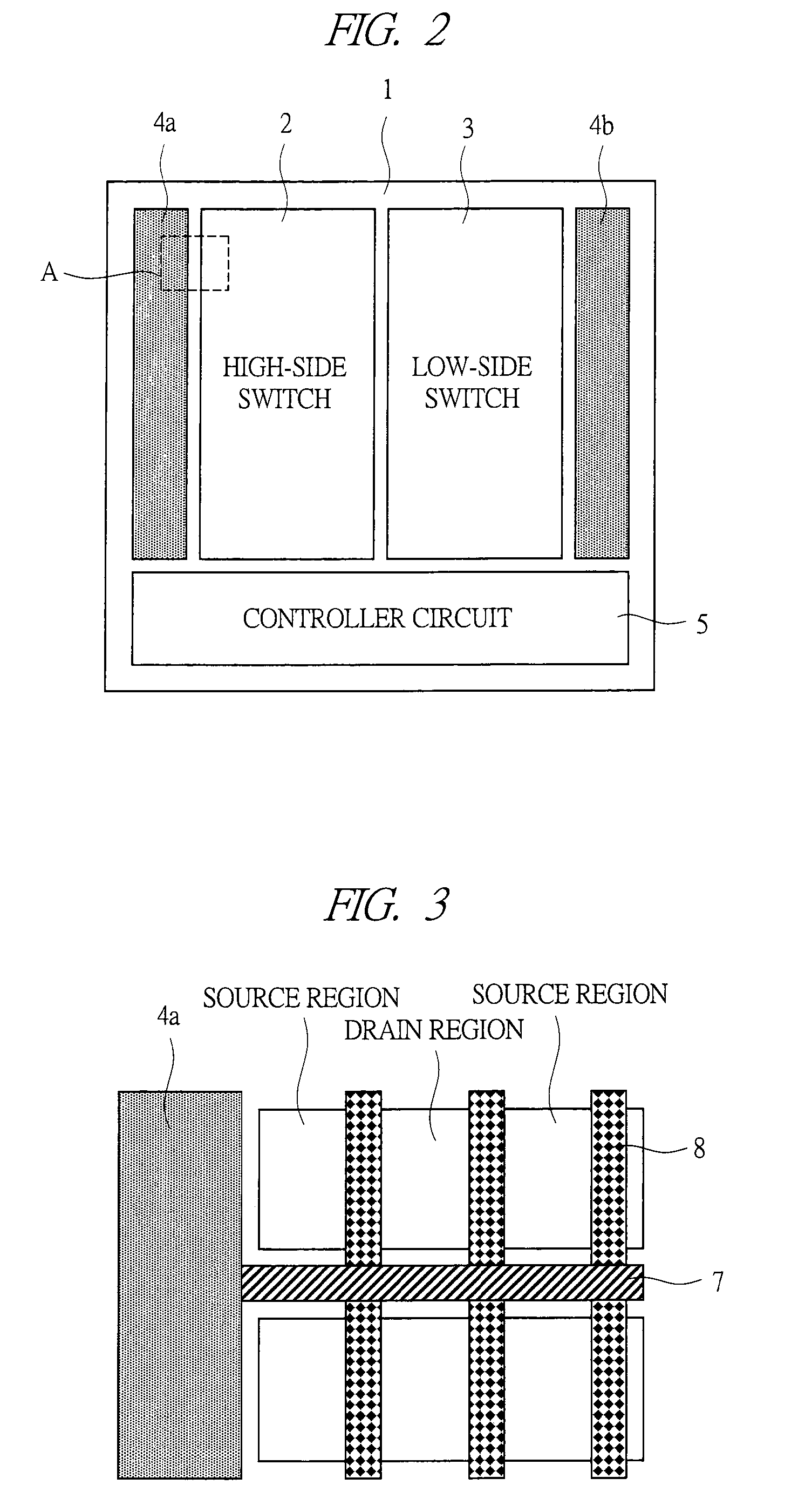
[0028]First, a semiconductor device according to a first embodiment of the present invention will be described with reference to FIG. 2. FIG. 2 is a layout view showing the semiconductor device according to the present embodiment. FIG. 2 is an illustration viewing the semiconductor device from a connecting portion side.
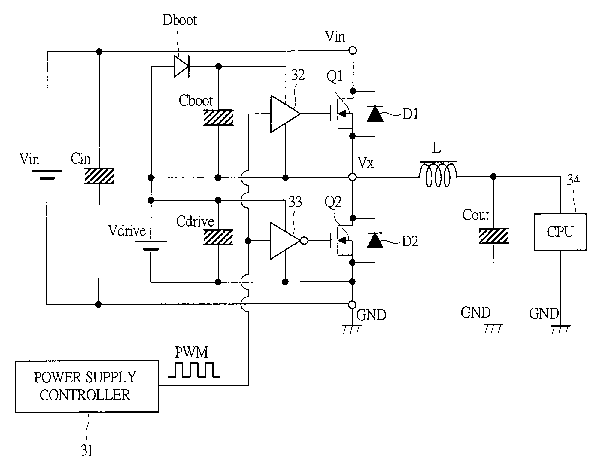
[0029]The semiconductor device according to the present embodiment is applied to a non-isolated DC-DC converter as shown in FIG. 1 described above. That is, the semiconductor device of the non-isolated DC-DC converter includes a high-side switch Q1, a high-side driver 32, a low-side switch Q2, and a low-side driver 33. The high-side switch Q1 is configured with a lateral MOSFET whose drain is connected to an input power supply Vin and whose source is connected to an output inductor L. The high-side driver 32 is a driver for driving the high-side switch Q1 and is connected to a gate of the lateral MOSFET of the high-side switch Q1. The low-side switch Q2 is configured with a lateral MOSFET whose drain is connected to the output inductor L and whose source is connected to a reference potential GND. The low-side driver 33 is a driver for driving the low-side switch Q2 and is connected to a gate of the lateral MOSFET of the low-side switch Q2.
[0030]In the semiconductor device according to the present embodiment, the lateral MOSFET is used for the high-side switch Q1 and the low-side switch Q2, and this advantage including a difference from a vertical MOSFET and the like will be described in detail in a third embodiment later.
[0031]Note that, in the correspondence relation between the layout view of FIG. 2 showing the semiconductor device according to the present embodiment and the circuit diagram of FIG. 1 described above, a high-side switch 2 corresponds to the high-side switch Q1 (diode D1: high-side built-in MOSFET), a high-side driver 4a corresponds to the high-side driver 32, a low-side switch 3 corresponds to the low-side switch Q2 (diode D2: low-side built-in MOSFET), a low-side driver 4b corresponds to the low-side driver 33, and a controller circuit 5 corresponds to the power supply controller 31, respectively, and they represent the same components.
[0032]As shown in FIG. 2, in the semiconductor device according to the present embodiment, the high-side switch 2 and the low-side switch 3, the high-side driver 4a for driving the high-side switch 2 and the low-side driver 4b for driving the low-side switch 3, and the controller circuit 5 for controlling the high-side driver 4a and the low-side driver 4b are mounted on a semiconductor substrate 1. More particularly, in the semiconductor device according to the present embodiment, the high-side driver 4a is arranged in a region closer to a periphery of the semiconductor substrate 1 than the high-side switch 2, and the low-side driver 4b is arranged in a region closer to the periphery of the semiconductor substrate 1 than the low-side switch 3. An n-type MOSFET or a p-type MOSFET is used as the high-side switch 2, and an n-type MOSFET is used as the low-side switch3. Although a circuit is simplified when the p-type MOSFET is used as the high-side switch 2 because the boot strap capacitor Cboot and the boot strap diode Dboot shown in FIG. 1 are unnecessary, the p-type MOSFET has a problem of high on-resistance, and therefore, the n-type MOSFET is used in many cases as the high-side switch 2 in a CPU power supply for which large current is required.
[0033]FIG. 3 shows an enlarged layout view of A region of FIG. 2. A gate electrode of an aluminum wire 7 is extended rightward from the high-side driver 4a in FIG. 3, and a gate electrode of a poly silicon wire 8 is extended so as to branch from the gate electrode of the aluminum wire 7, so that a source region and a drain region are arranged so as to interpose the gate electrode of the poly silicon wire 8. The MOSFET of the high-side switch 2 is configured with the gate electrode, the source region and the drain region interposing the gate electrode therebetween, and the like. The reason of using an aluminum wire for a long wire and a poly silicon wire for a short wire in wires of the gate electrodes is because a resistance of the aluminum wire is lower and the increase of the gate resistance can be suppressed even if the wires are long.
[0034]Next, the reason why the parasitic inductance can be reduced by the semiconductor device according to the present embodiment will be described with reference to FIG. 4. FIG. 4 is a layout view showing a printed board on which the semiconductor device according to the present embodiment is mounted.
[0035]FIG. 4 shows a state in which the semiconductor substrate 1 is stored in a semiconductor package 18 and they are flip-chip mounted on a printed board 11. Since the semiconductor substrate 1 is flip-chip mounted, right and left of the semiconductor substrate 1 are inverted with those of FIG. 2.
[0036]An input capacitor 12, a boot strap capacitor 13, and a drive capacitor 14 are arranged so as to surround the semiconductor package 18. Since the input capacitor 12 is arranged close to the high-side switch 2 and the low-side switch 3, a path from one terminal of the input capacitor 12 to the other terminal of the input capacitor 12 via the high-side switch 2 and the low-side switch 3 is short, so that the parasitic inductance can be reduced. Further, since the boot strap capacitor 13 is arranged close to the high-side driver 4a, a path from one terminal of the boot strap capacitor 13 to the other terminal of the boot strap capacitor 13 via the high-side driver 4a is short, so that the parasitic inductance can be reduced. Still further, since the drive capacitor 14 is arranged close to the low-side driver 4b, a path from one terminal of the drive capacitor 14 to the other terminal of the drive capacitor 14 via the low-side driver 4b is short, so that the parasitic inductance can be reduced. As a result, this leads to the improvement of the power conversion efficiency.
[0037]Note that, in the correspondence relation between the layout view of FIG. 4 and the circuit diagram of FIG. 1 described above, the input capacitor 12 corresponds to the input capacitor Cin, the boot strap capacitor 13 corresponds to the boot strap capacitor Cboot, and the drive capacitor 14 corresponds to the drive capacitor Cdrive, respectively.
[0038]FIG. 5 is a layout view showing a state where wires of the path from a positive terminal of the input power supply Vin to a negative terminal of the input power supply Vin via the high-side switch Q1 (2) and the low-side switch Q2 (3) are added to the printed board 11 of FIG. 4. As shown in FIG. 5, a power supply wire 15 connected to the positive terminal of the input power supply Vin and a reference potential wire (GND wire) 16 connected to the negative terminal of the input power supply Vin are arranged close to each other. This aims to cancel the magnetic flux caused in switching of the high-side switch 2 by arranging the power supply wire 15 and the reference potential wire 16 close to each other, thereby reducing the effective parasitic inductance. Meanwhile, it is not required to consider a parasitic inductance in an output wire 17 connected to the output inductor L. However, since reduction of its conversion efficiency due to the wire resistance is concerned, it is necessary to ensure a sufficiently large wire width.
[0039]FIG. 6 is a layout view describing a connecting portion between the semiconductor package 18 or the printed board 11 and the semiconductor substrate 1 on which the high-side switch 2, the low-side switch 3, and the controller circuit 5 are formed. FIG. 6 shows an example of using bumps 6 for the connection of the semiconductor substrate 1 on which the high-side switch 2, the low-side switch 3, and the controller circuit 5 are formed. The semiconductor substrate 1 is connected to the printed board 11 via the bumps 6. Also in a case of storing the semiconductor substrate 1 in the semiconductor package 18 and mounting them on the printed board 11, the semiconductor package 18 is connected to the printed board 11 via the bumps 6. As described above, in the present embodiment, the bumps 6 are used for the connecting portion in both of the semiconductor device in the state of the semiconductor substrate 1 and the semiconductor device in which the semiconductor substrate 1 is stored in the semiconductor package 18.
[0040]Conventionally, the wire bonding used for the connection between the semiconductor substrate 1 and the semiconductor package 18 has following problems. That is, an upper limit of the number of pins is low because bonding pads have to be provided in the periphery of the semiconductor substrate 1, and the wire resistance is high because the wires have to be led to the pads arranged in the periphery of the semiconductor substrate 1. Compared to this, since the bumps 6 can be the connecting portion in the whole semiconductor substrate 1, many pins can be provided. Also, since the connection is made from the center region of the semiconductor substrate 1 to the semiconductor package 18 or the printed board 11 via the bumps 6, the increase of the wire resistance caused by leading the wires of the semiconductor substrate 1 can be suppressed.
[0041]With regard to the arrangement of the bumps 6, for example, a layout example focusing on the potential as shown in FIG. 7 or that focusing on the electrodes as shown in FIG. 8 described later is possible.
[0042]FIG. 7 is a layout view arranged with focusing on the potential of the bumps of the high-side switch 2 and the low-side switch 3. As shown in FIG. 7, bumps 21 corresponding to the drain potential of the high-side switch 2 are connected to the positive terminal of the input power supply Vin, bumps 23 corresponding to the source potential of the high-side switch 2 and the drain potential of the low-side switch 3 are connected to one terminal of the output inductor L, and bumps 22 corresponding to the source potential of the low-side switch 3 are connected to the negative terminal of the input power supply Vin. In this case, the bumps 21 corresponding to the drain potential and the bumps 23 corresponding to the source potential are alternately arranged in a vertical direction in the high-side switch 2, and the bumps 22 corresponding to the source potential and the bumps 23 corresponding to the drain potential are alternately arranged in a vertical direction in the low-side switch 3. In this arrangement, the bumps 23 are arranged at the same positions in the high-side switch 2 and the low-side switch 3 when viewed in a vertical direction. By alternately arranging the bumps of the source and the drain as described above, the length of leading the wires of the semiconductor substrate 1 can be shortened, and the improvement of the conversion efficiency can be achieved.
[0043]FIG. 8 is a layout view arranged with focusing on the source electrodes and the drain electrodes of the bumps of the high-side switch 2 and the low-side switch 3. In FIG. 8, a symbol “S” indicates the source and a symbol “D” indicates the drain, respectively. As shown in FIG. 8, in the high-side switch 2, the bump of the source S and the bump of the drain D are alternately arranged in a lateral direction, and further, the bump of the source S and the bump of the drain D are alternately arranged also in a vertical direction. Similarly, also in the low-side switch 3, the bump of the source S and the bump of the drain D are alternately arranged in lateral and vertical directions. By alternately arranging the bumps of the source S and the drain D as described above, the length of leading the wires of the semiconductor substrate 1 can be shortened, and the improvement of the conversion efficiency can be achieved.
[0044]As described above, according to the present embodiment, in a semiconductor device in which the high-side switch 2, the high-side driver 4a, the low-side switch 3, the low-side driver 4b, and the like are formed on the same semiconductor substrate 1, the high-side driver 4a is arranged in a region closer to the periphery of the semiconductor substrate 1 than the high-side switch 2, and further, the low-side driver 4b is arranged in a region closer to the periphery of the semiconductor substrate 1 than the low-side switch 3, and therefore, the paths among the input capacitor 12, the boot strap capacitor 13, and the drive capacitor 14 are shortened. As a result, the parasitic inductance is reduced, and the conversion efficiency can be improved.
[0045]Further, according to the semiconductor device of the present embodiment, further improvement of the conversion efficiency is possible by devising the arrangement of the power supply wire 15 and the reference potential wire 16 and the arrangement of the output wire 17 and using the bumps 6 for the connecting portion and devising the arrangement of the bumps.