Current amplifying element and current amplification method

a current amplification and current technology, applied in the direction of galvano-magnetic amplifiers, galvano-magnetic devices, semiconductor devices, etc., can solve the problems of output waveform distortion, inability to perform amplification, delay in input output, etc., and achieve high speed

Inactive Publication Date: 2010-01-07
HIROSHIMA UNIVERSITY +1
View PDF1 Cites 1 Cited by
  • Summary
  • Abstract
  • Description
  • Claims
  • Application Information

AI Technical Summary

Benefits of technology

[0023]In the inventive current amplifying element, the input current path is located in a direction perpendicular to the magnetic field, the output current path is perpendicular to the input current path, and there is no factor that defines such a cutoff frequency's upper limit as is determined by the dependence of input impedance on frequency. Thus, the inventive current amplifying element is capable of operating at a very high speed.

Problems solved by technology

When the operating frequency is increased, this input impedance causes an input's output to be delayed, and at frequencies higher than a certain level, the output waveform is distorted or amplification cannot be performed.

Method used


Image

  • Current amplifying element and current amplification method
  • Current amplifying element and current amplification method
  • Current amplifying element and current amplification method

Examples


first embodiment

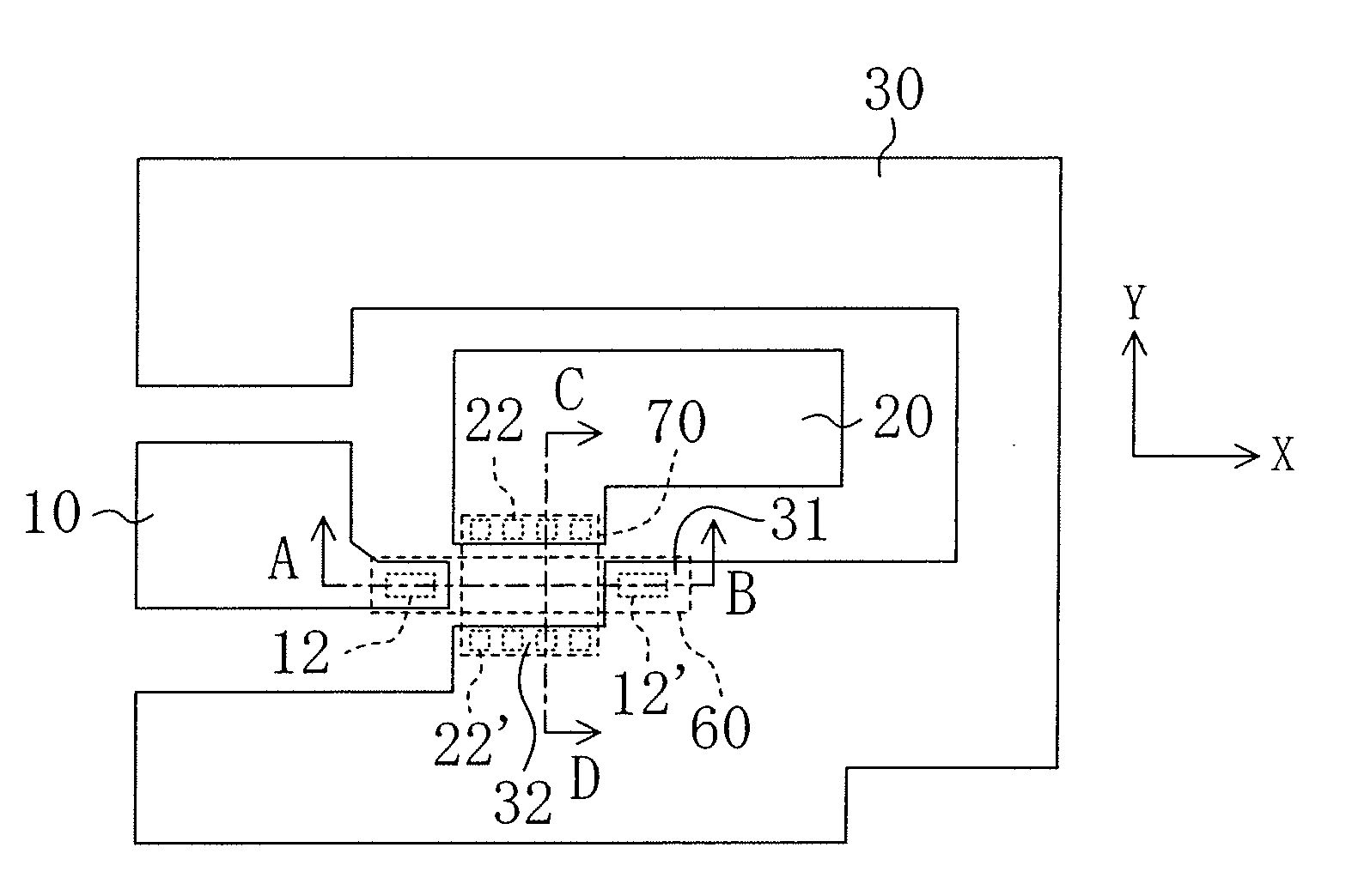
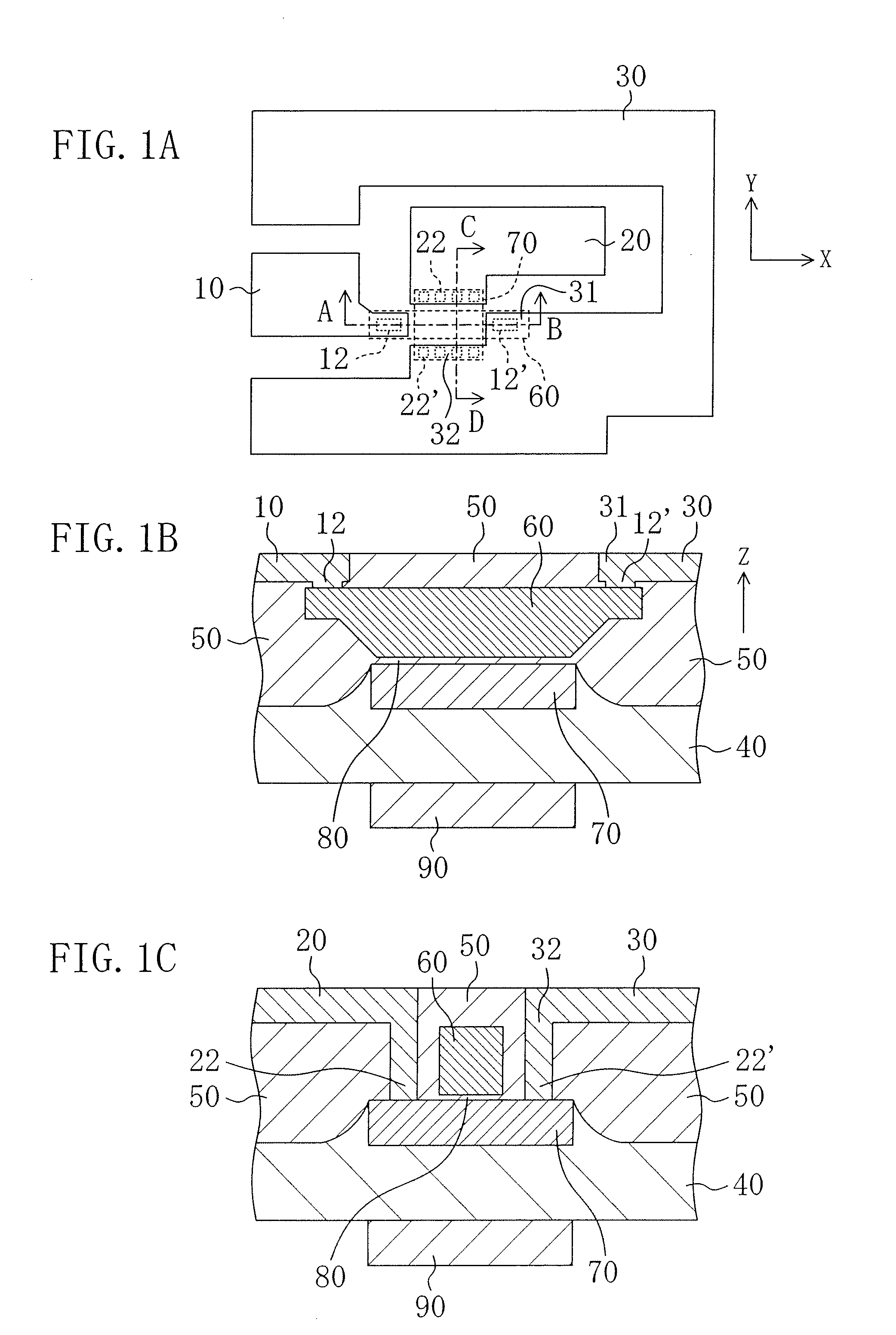
[0045]FIG. 1(a) is a schematic plan view of a current amplifying element according to a first embodiment, FIG. 1(b) is a schematic cross-sectional view taken along the line A-B in FIG. 1(a), and FIG. 1(c) is a schematic cross-sectional view taken along the line C-D in FIG. 1(a).

[0046]The current amplifying element of this embodiment is formed on a silicon substrate 40. In the cross-sectional views, i.e., in FIGS. 1(b) and 1(c), an input current path 60, which is made of polysilicon, is formed over an output current path 70, which is made of n+-type Si by doping, with an SiO2 insulator 80 interposed therebetween. A magnet 90 is bonded to the underside of the substrate 40. In the cross-sectional views, the magnet 90 has the north and south poles aligned in the vertical direction, and forms a magnetic field in the vertical direction (i.e., a direction Z) perpendicular to the output current path 70 and the input current path 60. The output current path 70 is a path (an area) where an ou...

example

[0056]The present inventors fabricated a current amplifying element having the same configuration as that shown in FIG. 1. The length (i.e., the distance between the input terminals) of the input current path 60 was 50 μm, and the length (i.e., the distance between the output terminals) of the output current path 70 was 0.1 μm. The thickness of the insulator 80 was 3.7 nm. A neodymium magnet having a magnetic flux density of 0.5 T was used as the magnet 90.

[0057]High frequency characteristics were evaluated by measuring the S parameters of the current amplifying element and then calculating from the S parameters an H21 component of the H parameters to obtain a current gain. The current gain is obtained as the magnitude |H21| of the H21 component. The input and output DC biases applied when the S parameters were measured were both 2V.

[0058]FIG. 3 shows the frequency characteristics of a current gain obtained by subtracting a current gain when no magnetic field was applied from a curr...

second embodiment

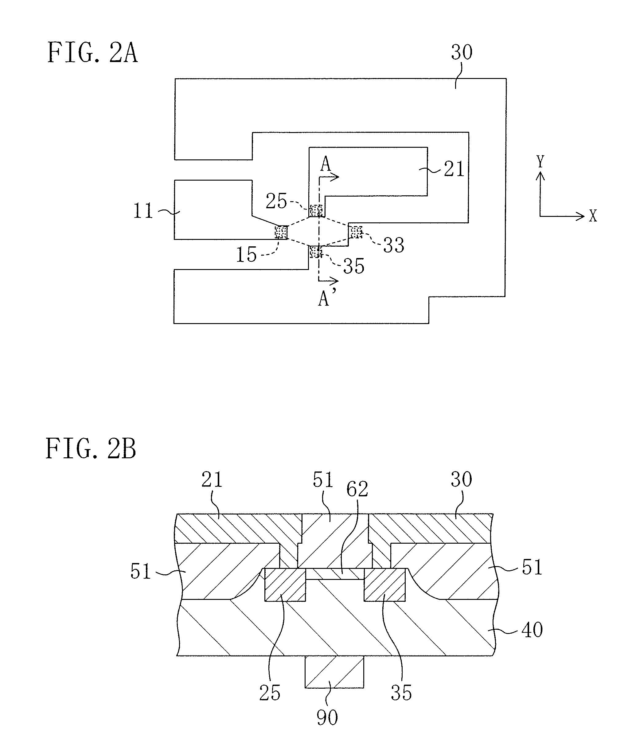
[0071]FIG. 2(a) is a schematic plan view of a current amplifying element according to a second embodiment, and FIG. 2(b) is a schematic cross-sectional view taken along the line A-A′ in FIG. 2(a).

[0072]The current amplifying element of this embodiment is formed on a silicon substrate 40, and an input current path and an output current path 62 are made of Si doped with an impurity. Unlike in the first embodiment, the input current path and the output current path 62 are not separated by an insulator, and parts of these current paths occupy the same part in the current amplifying element. Specifically, the input current path that connects two input terminals 15 and 33 (one of them is a part of a ground wire 30) and the output current path 62 that connects two output terminals 25 and 35 (one of them is a part of the ground wire 30) occupy the same area in the part shown in FIG. 2(b).

[0073]An input wire 11 made of Al is directly connected with the input current path at the input termina...


PUM


Abstract

A current amplifying element that operates at a higher speed than conventional semiconductor devices is provided. An input current flows through an input current path 60 in a direction X, and a magnetic field generated from a magnet 90 is applied in a direction Z which is perpendicular to the direction X. An output current path 70 is formed under the input current path 60 with an insulator 80 interposed therebetween. Since the direction in which an output current flows is perpendicular to both the input current and the magnetic field, the current is amplified by the galvanomagnetic effects produced by the input current and the magnetic field.

Description

TECHNICAL FIELD[0001]The present invention relates to a current amplifying element and a current amplification method, and more particularly, to a current amplifying element including a magnetic generator.BACKGROUND ART[0002]In recent years, the demand for high-capacity high-speed data transmission and reception has been increasing, and various studies are being undertaken to transmit and receive larger volumes of data at higher speeds. For example, to amalgamate electronics, which uses electronic devices such as field effect transistors, and photonics, which uses photonic devices such as light emitting diodes, signal processing techniques in the THz band which is in a higher frequency range than the millimeter wave band are being studied vigorously. To realize such techniques, electronic devices capable of operating in the THz band are indispensable.[0003]Of the electronic devices, transistors which perform amplification, e.g., MOS transistors, have a gate insulator and thus have i...

Claims


Application Information

Patent Timeline
Patent Type & Authority Applications(United States)
IPC IPC(8): H03F15/00
CPCH03F15/00H01L43/065H10N52/101H01L29/66H10N50/00
Inventor HIGUCHI, KATSUHIKOHIGUCHI, MASAHIKO
Owner HIROSHIMA UNIVERSITY
Why Eureka
Try Eureka