

Nitride based semiconductor device and fabrication method for the same
- Summary
- Abstract
- Description
- Claims
- Application Information
AI Technical Summary
Benefits of technology
Problems solved by technology
Method used
Image

Examples
first embodiment
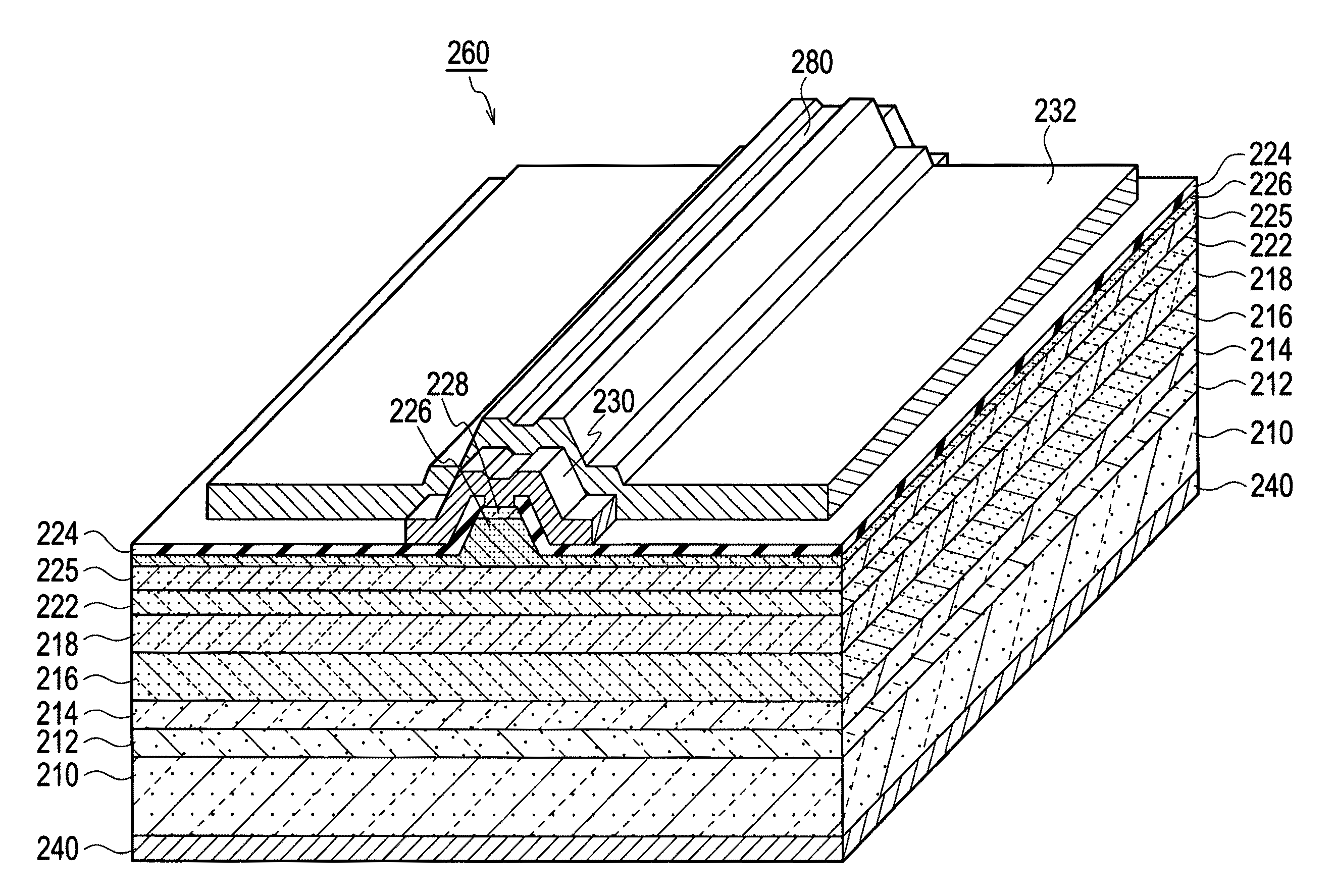
[0152]As schematically shown in the bird's-eye view of FIG. 8, a nitride based semiconductor device 20 according to a first embodiment of the present invention includes: a GaN based semiconductor substrate 10; an n-type GaN based buffer layer 12 placed on the GaN based semiconductor substrate 10; an n-type cladding layer 14 placed on the n-type GaN based buffer layer 12; an n-type GaN based guide layer 16 placed on the n-type cladding layer 14; an active layer 18 placed on the n-type GaN based guide layer 16; and a p-type GaN based guide layer 22 placed on the active layer 18. The n-type GaN based guide layer 16 is expressed by an n-type AlXInYGa1-X-YN (where 0<=X, 0<=Y, and X+Y<=1) layer.
[0153]Furthermore, the nitride based semiconductor device 20 according to the first embodiment includes: a first p-type cladding layer 26a placed at stripe shape on the p-type GaN based guide layer 22; an electron block layer 25 placed on the first p-type cladding layer 26a; a second p-type claddin...
second embodiment
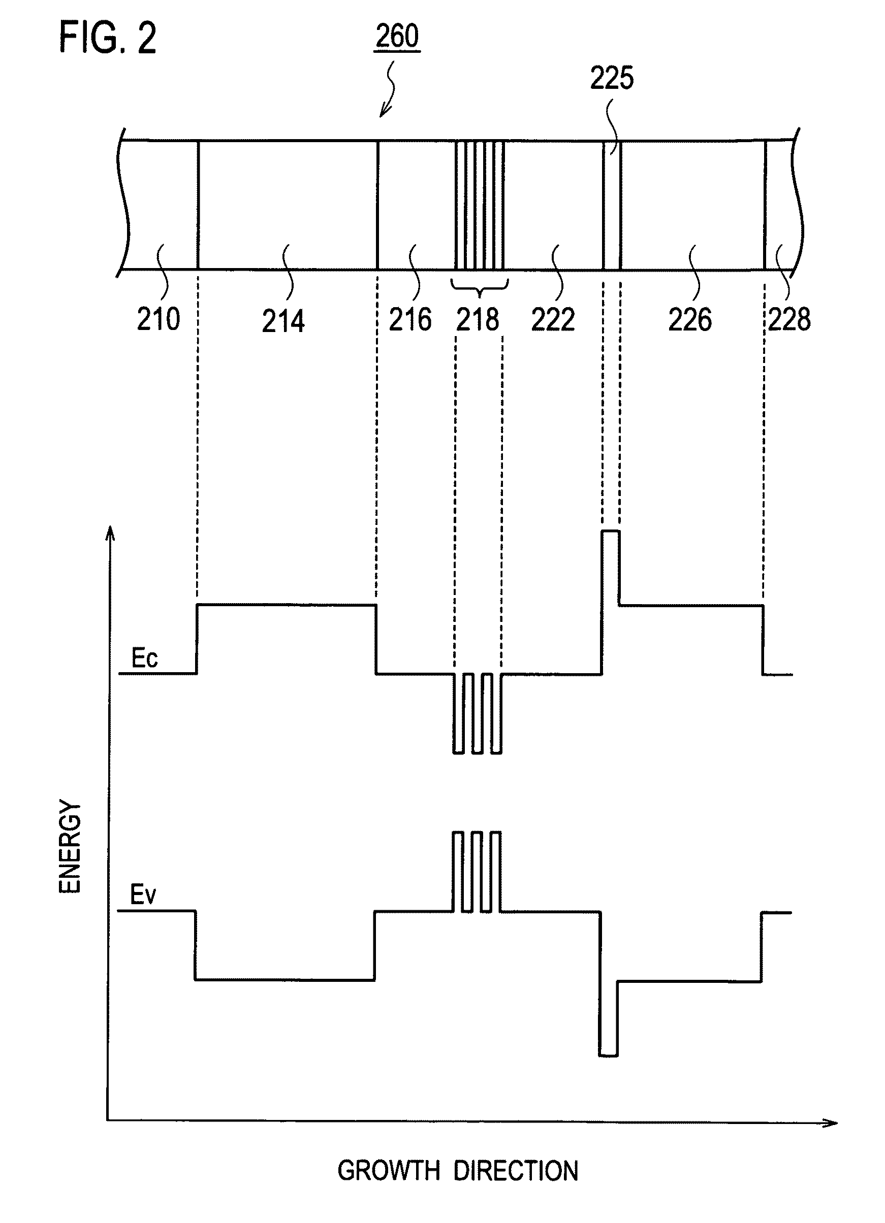
[0171]As schematically shown in the bird's-eye view of FIG. 12, a nitride based semiconductor device 20 according to a second embodiment of the present invention includes: a GaN based semiconductor substrate 10; an n-type GaN based buffer layer 12 placed on the GaN based semiconductor substrate 10; an n-type cladding layer 14 placed on the n-type GaN based buffer layer 12; an n-type GaN based guide layer 16 placed on the n-type cladding layer 14; an active layer 18 placed on the n-type GaN based guide layer 16; and a p-type GaN based guide layer 22 placed on the active layer 18.
[0172]Furthermore, the nitride based semiconductor device 20 according to the second embodiment includes an electron block layer 25 placed on the p-type GaN based guide layer 22, a stress relaxation layer 27 placed on the electron block layer 25, and a p-type cladding layer 26 placed on the stress relaxation layer 27.
[0173]The p-type cladding layer 26 is patterned and is removed by etching, and as shown in FI...
modified example 1
of the Second Embodiment
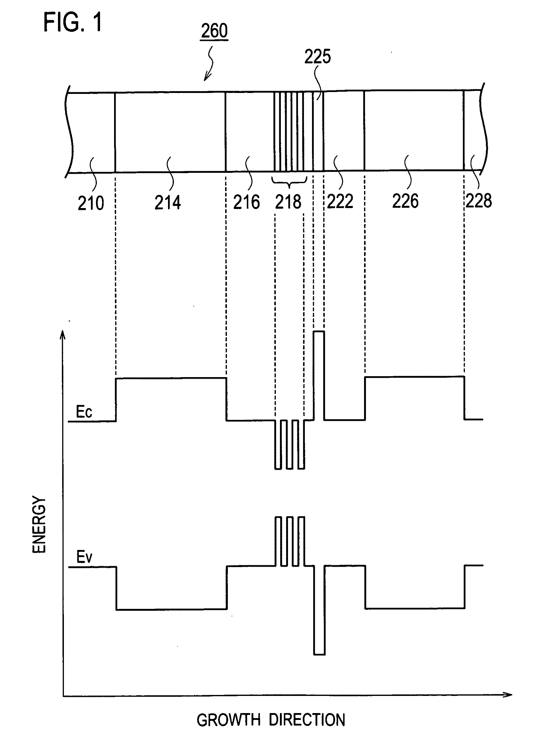
[0195]As shown in FIG. 14, as for an energy band structure of a nitride based semiconductor device according to a modified example 1 of the second embodiment, the electron block layer 25a has an energy potential structure of triangular shape. Since other structures are the same as that of the second embodiment, the explanation related to the structure of overlapping part is omitted.
[0196]In FIG. 14, the electron block layer 25a can be formed by the AlyGa1-yN layer (where 03 is about 3 nm to about 20 nm, and is about 7 nm to about 10 nm preferable, for example. The Al composition ratio y is continuously changed as it shifts to the interface T2, which contacts the stress relaxation layer 27 from the interface T1 which contacts the p-type GaN based guide layer 22. The composition inclination of Al composition is about 1.64 (% / nm), for example. If the thickness of the electron block layer 25 shall be about 14 nm, for example, the variation o...
PUM
 Abstract
Description
Claims
Application Information