Substrate holder

a technology of semiconductors and substrates, applied in the field of semiconductor holder, can solve the problems of unstable wafer temperature, inability to easily control the overall energy, and inability to accurately control the temperature of the substrate, and achieve the effects of easy contamination, accurate control of the substrate temperature, and high speed

Inactive Publication Date: 2010-01-21
CANON ANELVA CORP
View PDF3 Cites 18 Cited by
  • Summary
  • Abstract
  • Description
  • Claims
  • Application Information

AI Technical Summary

Benefits of technology

[0014]A technique in Japanese Patent Application Laid-Open No. 2004-087869 is used at a process temperature of 200° C. or less, and does not suppose control of the substrate temperature under a temperature condition of 200 to 500° C. In contrast, in techniques in Japanese Patent Application Laid-Open Nos. 10-303185 and 2000-299288, a substrate holder which is controlled to a set temperature ranging form 200 to 500° C. and which has a mechanism capable of performing heat exchange through a circulation medium for heat exchange is used. The substrate holder of this type is easily contaminated by leakage, adhesion, and the like of the circulation medium at the time of maintenance because the circulation medium is oil-based. The substrate holder is inconveniently handled in a clean room. The cooling medium (circulation medium) frequently has combustibility, and is used with a safety risk in a clean room.
[0015]The present invention has been made in consideration of the above circumstances, and an object of the invention is to provide a substrate holder which can accurately control a substrate temperature at a high speed within a temperature range of 200 to 500° C. while giving a waste heat emitting function for a heat input by a plasma or the like to a non-combustible cooling medium.

Problems solved by technology

For example, when the wafer temperature is to be controlled at a high temperature ranging from 200 to 500° C., due to a change in heat input energy by a plasma and heating or waste heat emission by the heater or the cooler of the base member, overall energy cannot be easily controlled, making the wafer temperature unstable.
Therefore, in response to a change in plasma heat input energy caused by a change of process conditions, a heat transfer coefficient cannot be easily controlled by adjusting the pressure of the heat transfer gas.
The wafer temperature is thus deteriorated in controllability.
In the temperature control method, the substrate temperature varies in the process processing step, and desired process performance cannot be disadvantageously obtained.
However, in the environment in which the heat input is transitional, the control response is poor because the thermal conductance is small.

Method used


Image

  • Substrate holder
  • Substrate holder
  • Substrate holder

Examples


first embodiment

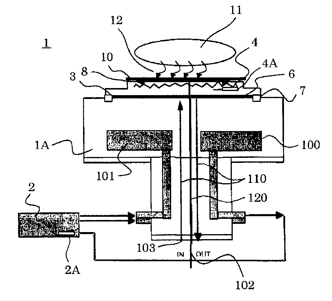
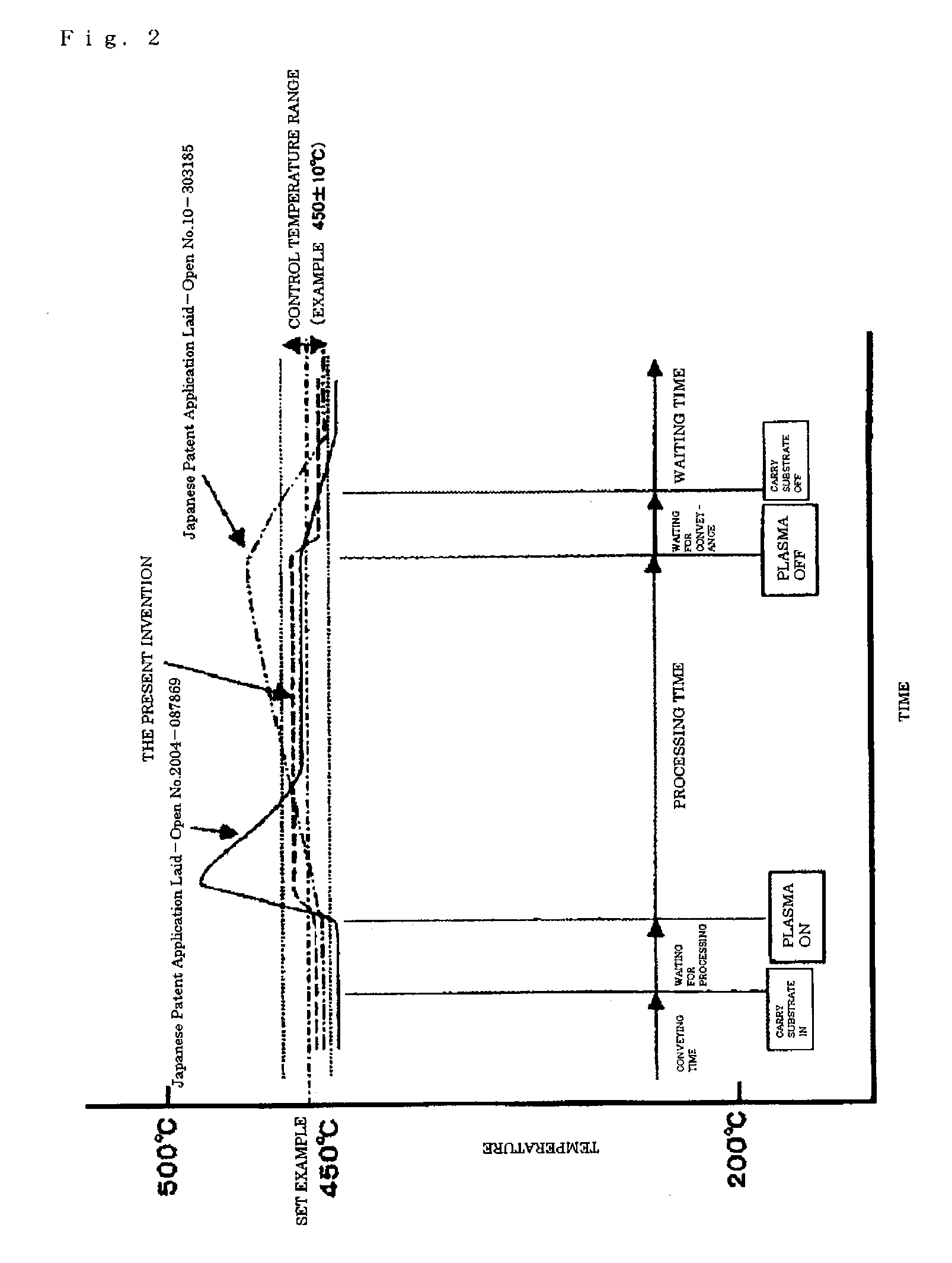
[0028]FIG. 1 is a schematic diagram showing a first embodiment of a substrate holder according to the present invention. FIG. 2 is a diagram for explaining a change in temperature of the substrate holder according to the present invention in relation to a conventional change in temperature.

[0029]As shown in FIG. 1, a substrate holder 1 according to the first embodiment is arranged in a vacuum vessel (not shown) of a plasma processing apparatus typified by a sputtering apparatus. The substrate holder 1 holds a substrate 10 on an electrostatic chuck 3 arranged on a substrate holding side (upper portion) of a holder main body 1A by electrostatic adsorption.

[0030]The holder main body 1A is, for example, a disk-like or columnar support member which supports a semiconductor wafer serving as the substrate 10. A circulation medium distribution path 100 to cause a circulation medium (cooling medium) 101 to flow is partitioned and formed inside the holder main body 1A. A circulation medium su...

second embodiment

[0045]FIG. 3 is a schematic diagram showing a substrate holder according to a second embodiment. FIG. 4 is a sectional view showing a transverse sectional structure of a heat transference varying unit in the second embodiment. In the second embodiment, the same members as those in the first embodiment will be given the same reference numerals as in the first embodiment.

[0046]A substrate holder 21 according to the second embodiment is obtained by changing the structure of the heat transference varying unit 6 partitioned and formed in the gap between the holder main body 1A and the electrostatic chuck 3 in a substrate holder having the same specification as that of the first embodiment.

[0047]More specifically, the heat transference varying unit 6 according to the second embodiment is partitioned and formed such that a first plate-like member 16 and a second plate-like member 17 which have circular-arc fins 16A and 17A standing upright on counter surfaces, respectively, are arranged to...

third embodiment

[0049]FIG. 5 is a schematic diagram showing a third embodiment of the semiconductor holder according to the present invention. FIG. 2 is a diagram for explaining a change in temperature of the substrate holder according to the present invention in relation to a conventional change in temperature.

[0050]As shown in FIG. 5, the substrate holder 1 according to the third embodiment is arranged in a vacuum vessel (not shown) of a plasma processing apparatus typified by a sputtering apparatus. The substrate holder 1 holds the substrate 10 on the electrostatic chuck 3 arranged on a substrate holding side (upper portion) of the holder main body 1A by electrostatic adsorption.

[0051]The holder main body 1A is, for example, a disk-like or columnar support member which supports a semiconductor wafer serving as the substrate 10. The circulation medium distribution path 100 to cause the circulation medium (cooling medium) 101 to flow is partitioned and formed inside the holder main body 1A. The ci...


PUM

PropertyMeasurementUnit
widthaaaaaaaaaa
heat transfer coefficientaaaaaaaaaa

Abstract

A substrate holder which has an electrostatic chuck on a substrate holding side of a holder main body and electrostatically adsorbs a substrate includes: a heating unit which is built in the electrostatic chuck and heats the substrate; a circulation medium distribution path which is formed inside the holder main body and connected to a circulation medium supplying unit which circulates and supplies a circulation medium; a heat transference varying unit which is formed by sealing a heat transfer gas in a gap between the holder main body and the electrostatic chuck and connected to a heat transfer gas supply system which can control a sealing pressure; and a gas sealing unit which is formed by sealing a heat transfer gas in a gap between the electrostatic chuck and the substrate and connected to the heating transfer gas supply system.

Description

BACKGROUND OF THE INVENTION[0001]1. Field of the Invention[0002]The present invention relates to a semiconductor holder which holds a substrate in a vacuum vessel of a plasma processing apparatus by electrostatic adsorption to make it possible to control a substrate temperature.[0003]2. Description of the Related Art[0004]A substrate holder (substrate supporting apparatus) which holds a substrate (wafer) is arranged in a vacuum vessel of a plasma processing apparatus such as a sputtering apparatus or an etching apparatus, and a substrate temperature is generally controlled.[0005]For example, a substrate supporting apparatus including a base member which has a heater or a cooler built therein and an electrostatic chuck which adsorptively holds a wafer on an upper portion of the base member through a heat transfer sheet is proposed (see Japanese Patent Application Laid-Open No. 2001-110883). In the base member, a gas feeding path which feeds a heat transfer gas is formed, and a gas ac...

Claims


Application Information

Patent Timeline
Patent Type & Authority Applications(United States)
IPC IPC(8): H01L21/683C23C16/458H01L21/465
CPCC23C14/50C23C16/4586H01L21/6831H01L21/67109C23C16/466
Inventor TATSUHIKO, YOSHIDAKAZUAKI, KANEKOYOH, TANAKA
Owner CANON ANELVA CORP
Why Eureka
Try Eureka