Realizing N-Face III-Nitride Semiconductors by Nitridation Treatment

a technology of nitride and semiconductors, applied in the direction of semiconductor devices, basic electric elements, electrical equipment, etc., can solve the problems of ineffective attack of gallium layers, unable to obtain bulk crystals of gans, and disadvantages of existing gan formation processes, etc., to achieve the effect of reducing nitrogen vacancies in iii-nitride layers and increasing carrier concentrations

Inactive Publication Date: 2010-01-21
TAIWAN SEMICON MFG CO LTD
View PDF12 Cites 19 Cited by
  • Summary
  • Abstract
  • Description
  • Claims
  • Application Information

AI Technical Summary

Benefits of technology

[0011]The advantageous features of the present invention include the conversion of Ga-faced III-nitride layers to N-faced, so that wet etching may be used to pattern III-nitride layers. Furthermore, the nitrogen vacancies in the III-nitride layers may be reduced, resulting in increased carrier concentrations in the p-type III-nitride layers.

Problems solved by technology

Due to the high equilibrium pressure of nitrogen at typical growth temperatures, it is extremely difficult to obtain GaN bulk crystals.
The existing GaN formation process, however, suffers from drawbacks.
However, due to the significant difference in the etching characteristics between the gallium layer and the GaN layer, the etchant commonly used for patterning GaN layers, for example, KOH solution, may not be able to attack the gallium layer efficiently.
Therefore, instead of using the wet etch that has a greater throughput, dry etch has to be used for patterning the GaN layer, resulting in reduced throughput.
However, this method results in a silicon nitride layer being formed on the silicon substrate.
Due to the amorphous structure of the silicon nitride layer, the crystalline structure of the subsequently formed GaN layer is adversely affected.
Further, silicon nitride is not conductive, and hence bottom electrodes cannot be formed on the backside of the substrate.
An additional problem is that the GaN layer often has a relatively great concentration of nitrogen vacancies.

Method used


Image

  • Realizing N-Face III-Nitride Semiconductors by Nitridation Treatment
  • Realizing N-Face III-Nitride Semiconductors by Nitridation Treatment
  • Realizing N-Face III-Nitride Semiconductors by Nitridation Treatment

Examples


Embodiment Construction

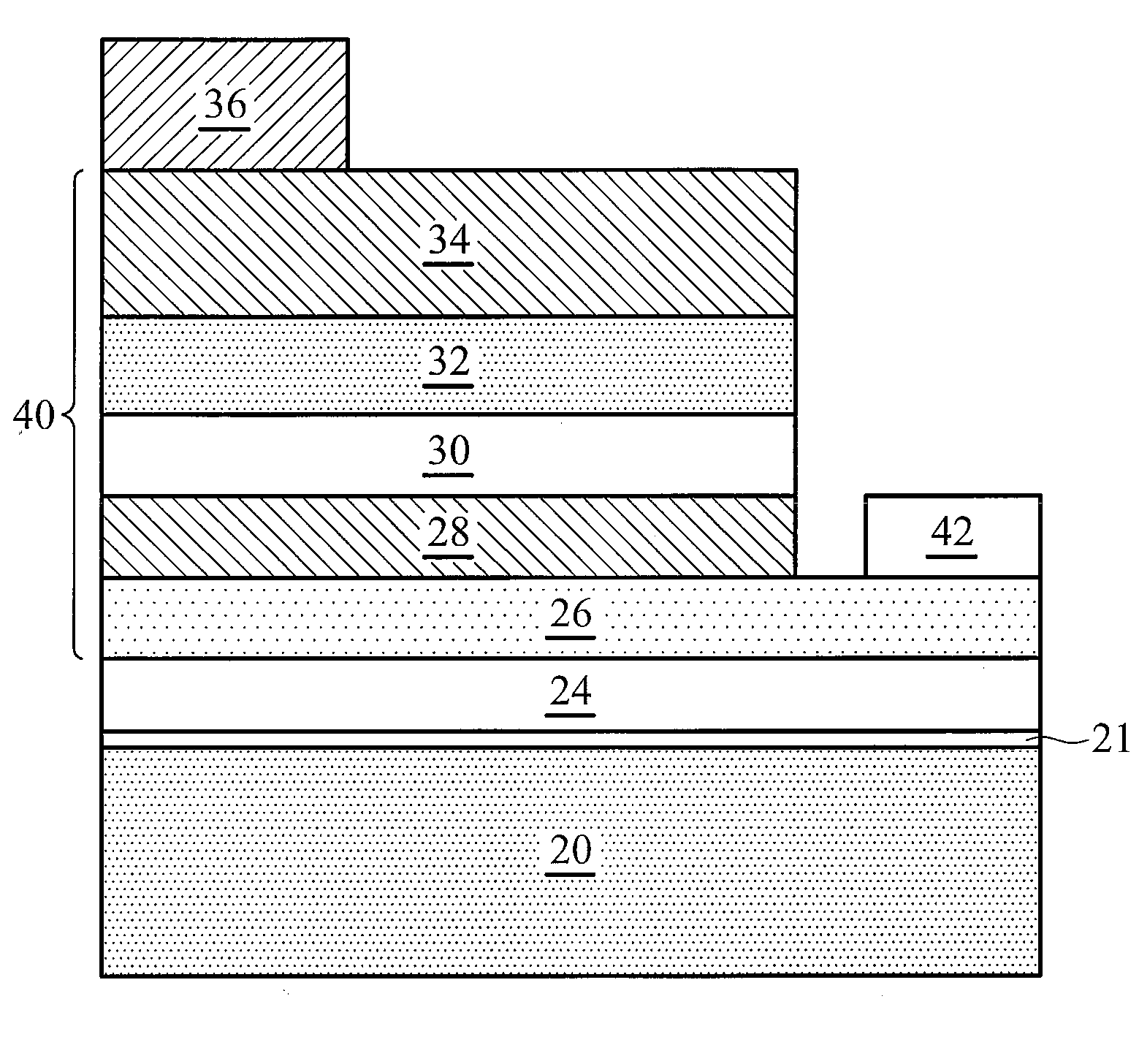
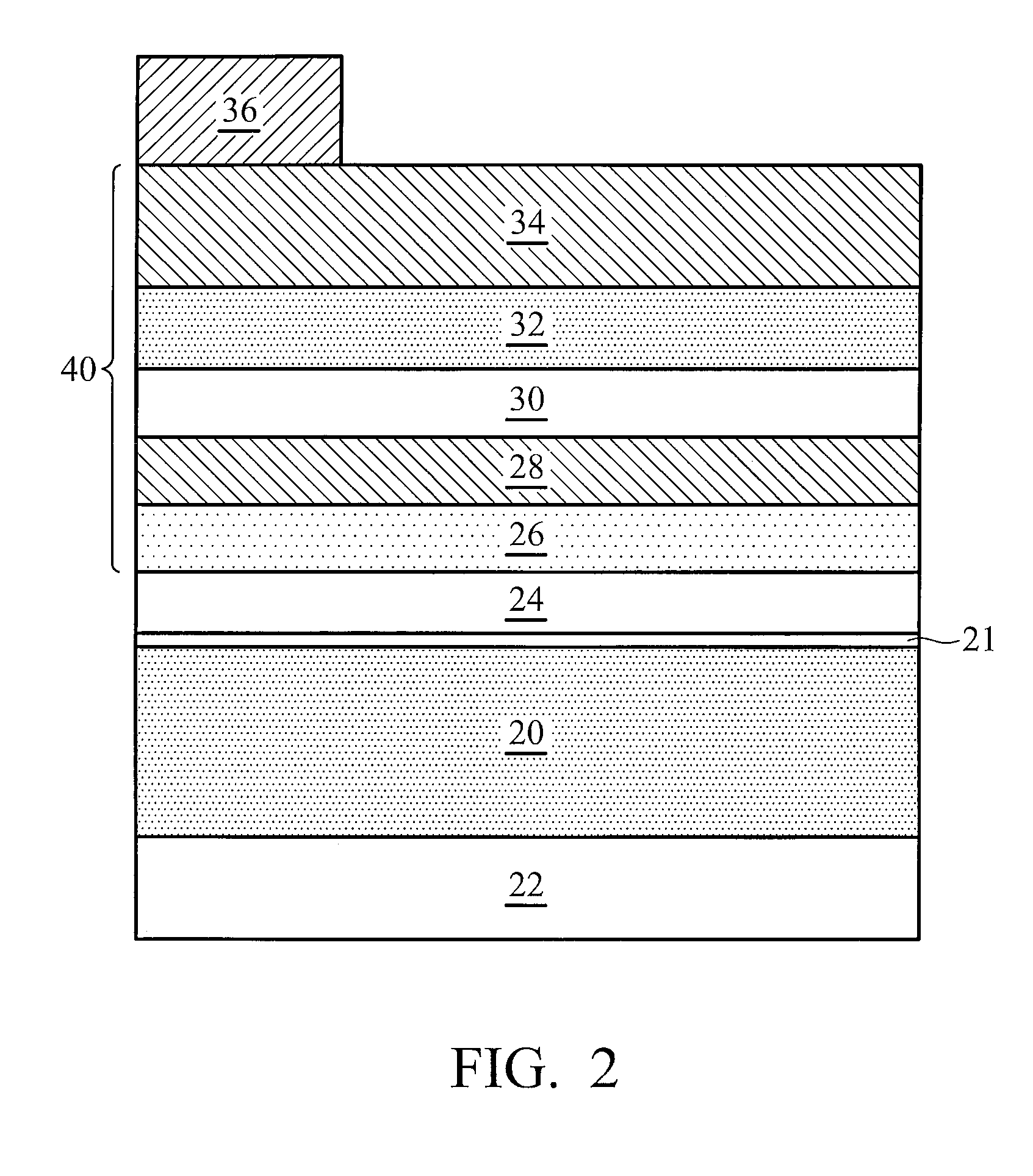
[0015]The making and using of the presently preferred embodiments are discussed in detail below. It should be appreciated, however, that the present invention provides many applicable inventive concepts that can be embodied in a wide variety of specific contexts. The specific embodiments discussed are merely illustrative of specific ways to make and use the invention, and do not limit the scope of the invention.

[0016]A novel method for forming semiconductor structures comprising group-III nitride (often referred to as III-nitride, or III-N) compounds is provided. The intermediate stages of manufacturing preferred embodiments of the present invention are discussed. Throughout the various views and illustrative embodiments of the present invention, like reference numbers are used to designate like elements.

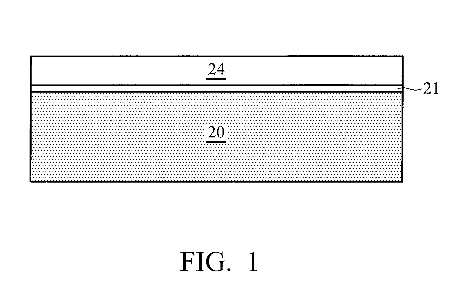
[0017]Referring to FIG. 1, substrate 20 is provided. In an embodiment, substrate 20 is a conductive (or semi-conductive) substrate comprising GaN, Si, Ge, SiGe, SiC, ZnO, SnS, SnSe,...


PUM

PropertyMeasurementUnit
temperatureaaaaaaaaaa

Abstract

A method of forming a semiconductor structure includes providing a substrate; forming a buffer/nucleation layer over the substrate; forming a group-III nitride (III-nitride) layer over the buffer/nucleation layer; and subjecting the III-nitride layer to a nitridation. The step of forming the III-nitride layer comprises metal organic chemical vapor deposition.

Description

[0001]This application claims priority to U.S. Provisional Patent Application Ser. No. 61 / 082,428, filed Jul. 21, 2008, and entitled “Realizing N-Face III-Nitride Semiconductors by Nitridation Treatment,” which application is hereby incorporated herein by reference.TECHNICAL FIELD[0002]This invention relates generally to semiconductor device manufacturing processes, and more particularly to forming group-III nitride films, and even more particularly to forming group-III nitride films on silicon substrates.BACKGROUND[0003]Group-III nitride (often referred to as III-nitride, or III-N) compounds, such as gallium nitride (GaN) and its related alloys, have been under intense research in recent years due to their promising applications in electronic and optoelectronic devices. Particular examples of potential optoelectronic devices include blue light emitting diodes and laser diodes, and ultra-violet (UV) photo-detectors. The large bandgap and high electron saturation velocity of the III-...

Claims


Application Information

Patent Timeline
Patent Type & Authority Applications(United States)
IPC IPC(8): H01L21/205
CPCH01L21/0237H01L21/02458H01L21/02664H01L21/02573H01L21/02617H01L21/0254
Inventor YU, CHEN-HUAYU, CHIA-LINCHEN, DING-YUANCHIOU, WEN-CHIH
Owner TAIWAN SEMICON MFG CO LTD
Why Eureka
Try Eureka